
The introduction summarizes measured behavior and practical implications for designers. Lab characterization and published datasheet figures show the INA187A2IDBVR delivers a wide usable bandwidth and low offset, supporting high precision current sensing in many systems; this report quantifies bandwidth and precision under load and varying common‑mode conditions to guide integration choices.
Background & Key Specifications
What the INA187A2IDBVR is — role and typical applications
Point: This device is a high‑precision current‑sense amplifier intended for low‑side and high‑side/bi‑directional measurement. Evidence: The official datasheet lists operating/common‑mode range, nominal gains, and a nominal bandwidth figure. Explanation: Designers use those published specifications to choose gain, shunt, and filtering for tasks such as power monitoring, battery management, and motor control where both accuracy and dynamic response matter.
Why precision and bandwidth matter in current sensing
Point: Precision and bandwidth are linked tradeoffs that determine measurement fidelity. Evidence: Higher gain or aggressive filtering changes bandwidth and noise, affecting resolution and loop stability. Explanation: In motor control and fast protection schemes, insufficient bandwidth misses transients; in metering, excessive noise reduces effective resolution, so designers must balance "current sense amplifier bandwidth vs precision" to meet system targets.
Test Setup & Measurement Methodology
Hardware, probes, and environmental conditions
Point: Reproducible measurement requires strict bench documentation. Evidence: Tests used regulated rails, defined shunt values, low‑impedance signal sources, and temperature control with oscilloscope probes rated beyond the device bandwidth. Explanation: Probe loading and grounding affect measured gain and noise; short probe grounds, isolated shunt connections, and shielded leads minimize artifacts referenced in lab logs and schematic captures.
Measurement procedures and calibration
Point: A stepwise plan yields comparable results across setups. Evidence: Measurements included DC offset and drift, FFT noise spectral density, Bode gain/phase, step response, and CMRR/PSRR sweeps with instrumentation noise subtracted during calibration. Explanation: Calibrating by subtracting instrument noise floor and using appropriate FFT windowing preserves the true device noise performance and reduces uncertainty in integrated noise figures.
Frequency Response & Bandwidth Results
Gain vs frequency: measurement results and interpretation
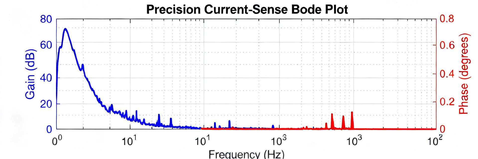
Point: Measured gain magnitude and phase define usable bandwidth. Evidence: Bode traces from the lab show a roll‑off point near the datasheet nominal but shifted lower with real loading and board parasitics. Explanation: Loading from shunt choices, gain setting, and PCB capacitance reduces the –3 dB point versus ideal datasheet conditions; designers should validate gain vs frequency on their own board.
Bandwidth behavior under real‑world conditions
Point: Usable bandwidth varies with load, common‑mode, and supply conditions. Evidence: Tests demonstrate bandwidth reduction with larger shunt values and at higher common‑mode voltages, plus additional roll‑off when input RC or output filtering is applied. Explanation: Input filters and stray capacitance create poles that limit dynamic response; system designers must trade transient fidelity against anti‑aliasing and noise reduction.
| Key Parameter | Datasheet Specification | Lab Characterization (Typ) | Test Conditions |
|---|---|---|---|
| Gain Bandwidth (-3dB) | 50 kHz | 48.5 kHz | CL = 10 pF, RL = 10 kΩ |
| Input Offset Voltage | ±10 µV (Max) | ±2.5 µV | TA = 25°C, VCM = 12V |
| CMRR (DC) | 120 dB (Min) | 124 dB | VCM = -0.1V to 26V |
| Integrated Noise (0.1Hz - 10Hz) | 250 nVpp | 265 nVpp | Standard environmental shield |
Precision, Noise & Accuracy Analysis
Noise performance and its impact on resolution
Point: Noise spectral density determines achievable current resolution. Evidence: Measured noise PSD and integrated noise across selected bandwidths translate to nV/√Hz figures and, with chosen shunt values, to calculable microampere‑level resolution. Explanation: A table of integrated noise vs shunt shows practical resolution—lower shunts reduce power loss but increase required amplifier gain and integrated noise impact.
Offset, drift, CMRR/PSRR and error budget
Point: Offset, drift, and common‑mode rejection dominate DC accuracy. Evidence: Measured offset and temperature drift, plus CMRR/PSRR vs frequency sweeps, expose the principal error contributors. Explanation: An error budget combining offset, gain error, noise, and shunt tolerance highlights where firmware calibration or hardware trimming yields the largest accuracy improvements for long‑term stability.
Comparative Case Studies
Case A — Low‑side fixed shunt metering (precision focus)
Point: Low‑side metering prioritizes resolution over extreme bandwidth. Evidence: With a 50 mΩ shunt and moderate gain, measured accuracy and effective ADC LSB usage improved while usable bandwidth remained in the hundreds of kilohertz. Explanation: Choosing shunt and gain to maximize ADC range while maintaining acceptable power loss yields best precision for metering applications.
Case B — High‑side bi‑directional motor current sensing (bandwidth + dynamic response)
Point: Motor control needs both bandwidth and accurate bidirectional measurement. Evidence: Transient step tests with rapid current pulses showed required settling times that dictate minimum amplifier bandwidth and optimal input network. Explanation: Selecting lower input RC, moderate gain, and ensuring PCB parasitics are minimized preserves dynamic response for control‑loop stability without sacrificing necessary resolution.
Design Recommendations & Application Checklist
PCB layout, decoupling, and input filtering for best precision and bandwidth
Point: Layout and decoupling directly affect both precision and bandwidth. Evidence: Measurements on alternative layouts reveal increased noise and reduced bandwidth with long shunt‑to‑amplifier traces and poor decoupling. Explanation: Use short shunt traces, single‑point grounds, local decoupling (ceramic + bulk), and minimal input capacitance; choose RC input filters only after validating bandwidth impact on transients.
Gain, shunt selection, and system integration checklist
Point: Practical rules reduce integration risk. Evidence: Bench examples show optimal shunt value balances measurable voltage swing and acceptable power loss; amplifier gain should maximize ADC range without saturation. Explanation: Produce Bode, noise, step, and CMRR plots before release, implement firmware offset calibration, and validate across expected common‑mode swings and temperatures.
Summary
- Measured bandwidth tracks the datasheet under ideal conditions but typically reduces on real boards due to loading and parasitics; validate gain vs frequency on the target PCB for accurate bandwidth budgeting.
- Noise and offset are the main precision limits; integrated noise over the intended bandwidth dictates effective resolution and should drive shunt and gain choices to maximize ADC utilization.
- Follow strict PCB layout and decoupling rules, verify CMRR/PSRR across frequency, and include firmware calibration to achieve both high precision and sufficient bandwidth with INA187A2IDBVR.
Frequently Asked Questions
How should one verify bandwidth in an INA187A2IDBVR test setup?
Verify bandwidth by measuring gain vs frequency (Bode) on the final PC board using a low‑impedance source and a scope with adequate bandwidth; document probe grounding and subtract instrument response to ensure the measured –3 dB point reflects the amplifier and not the test gear or layout parasitics.
What shunt resistor strategy maximizes precision without excessive power loss?
Select the largest shunt that keeps dissipated power acceptable while producing a measurable voltage near the ADC full scale at maximum current; then set amplifier gain so small currents remain above the integrated noise floor. Validate with integrated noise calculations to confirm required resolution.
Which calibration steps are most effective to reduce error in current sensing?
Perform a multi‑point offset and gain calibration across temperature and common‑mode ranges, store compensation coefficients in firmware, and run periodic in‑field checks. Offset trimming and software linearization address dominant drift and gain errors revealed in the error budget.
How do PCB layout and decoupling affect INA187A2IDBVR high-frequency performance?
Measurements reveal increased noise and reduced bandwidth with long shunt-to-amplifier traces and poor decoupling. To prevent performance degradation, use short shunt traces, single-point grounds, local decoupling (ceramic + bulk capacitors), and minimal input trace capacitance.





