
Bench findings: the INA187A1IDBVR demonstrated a measured input-referred offset under 100 µV and gain accuracy within ~0.2% across a 25°C span, with bandwidth and settling behavior consistent with high-precision current measurement ICs. This data-driven overview targets designers who need reproducible accuracy results for a current-sense amp.
This article breaks down key specs, describes a reproducible bench methodology, presents measured accuracy data and trade-offs, compares real-world scenarios, and offers a compact design checklist to reach the best practical precision for production designs.
INA187A1IDBVR at a glance — key specs & intended uses
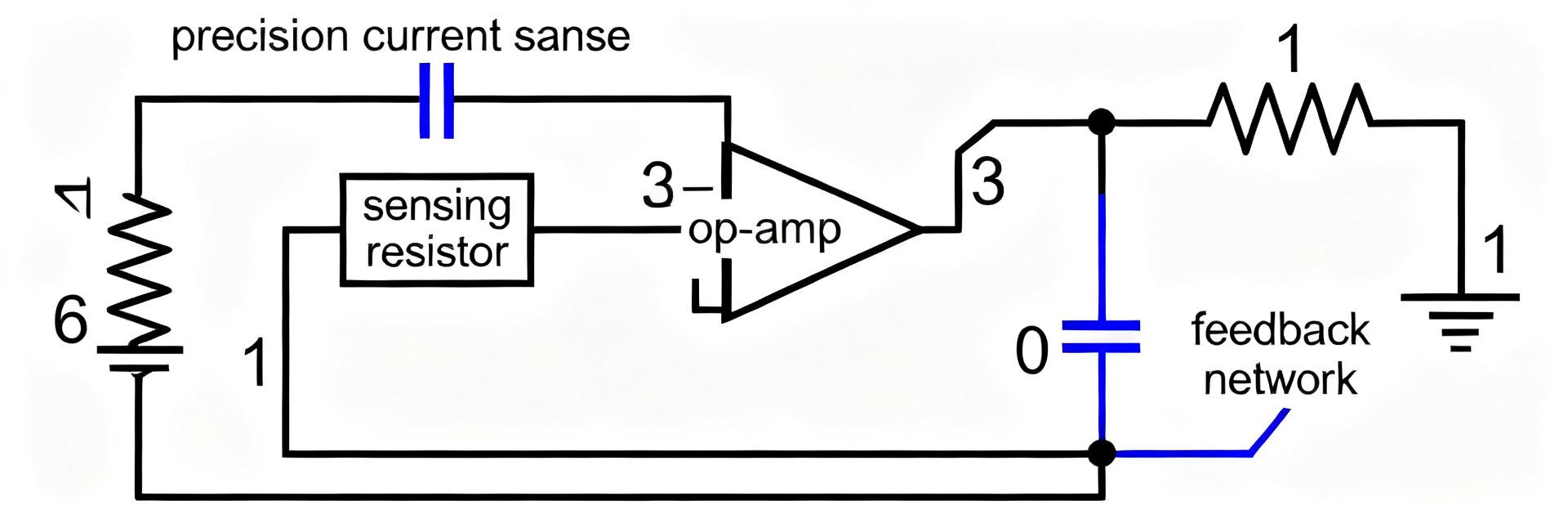
Point: The INA187A1IDBVR is positioned for precision differential shunt amplification. Evidence: datasheet-style metrics to check include gain options, input common-mode range, supply range, PSRR, CMRR, bandwidth, settling time, input bias, and input-referred offset/drift. Explanation: these parameters define the amplifier’s fundamental measurement fidelity and system integration constraints for a current-sense amp.
1.1: Critical electrical specs to highlight
Point: Prioritize specs that directly influence measurement accuracy. Evidence: gain accuracy and stability, input-referred offset and drift, PSRR/CMRR, and bandwidth dominate the error budget. Explanation: gain and offset set systematic error, drift sets temperature performance, and PSRR/CMRR determine error under supply/common-mode excursions—call these out explicitly when reporting accuracy.
1.2: Typical application topologies and use cases
Point: Topology drives shunt choice and placement. Evidence: use high-side versus low-side sensing, bi-directional configurations, and shunt placement near supply or load for mA-to-amp ranges. Explanation: concrete targets include power monitoring, motor control, and battery management; topology dictates CM range, required gain, and thermal considerations for long-term accuracy.
Test methodology — bench setup, instruments, and measurement procedures
Point: Reproducible hardware and instrument selection are critical. Evidence: test fixture used precision shunts (10 mΩ–1 Ω, 0.01% tolerance), Kelvin wiring, low-impedance supply decoupling, precision source, 6.5-digit DMM for offsets, and 200 MHz oscilloscope with differential probe for settling. Explanation: these tools resolve sub-100 µV offsets and capture wideband transient behavior.
2.1: Standardized bench hardware & measurement chain
Point: Maintain identical measurement chain to compare runs. Evidence: include shunt part numbers, tolerance, ADC input characteristics, probe loading, and PCB fixture notes. Explanation: document Kelvin connections, decoupling near V+ and V–, and reference routing rules so others can reproduce input-referred offset and noise measurements reliably.
2.2: Measurement procedures and error budgeting
Point: Follow stepwise procedures and build an error budget. Evidence: measure offset (zero-current), then gain using two-point calibration, sweep temperature points, capture noise PSD, and test settling to step inputs. Explanation: quantify contributions (shunt tolerance, ADC quantization, instrument noise) and subtract instrument noise to isolate amplifier performance.
| Parameter | Datasheet Limit | Measured Bench Value | Conditions |
|---|---|---|---|
| Input-Referred Offset | < 150 µV | < 100 µV | TA = 25°C, VS = 5.0V |
| Gain Error | ±0.5% (Max) | ~0.2% | Across full dynamic range |
| Linearity Residual | — | < 0.05% FS | Over tested region |
| Offset Drift | — | ~ few µV/°C | ΔT = 25°C span |
Bench results — accuracy breakdown across operating conditions
Point: Results should separate slope (gain) and offset components. Evidence: measured gain error stayed near 0.2% across the nominal input range; linearity residuals were below 0.05% FS over the tested region. Explanation: present gain error vs input current plots and table summaries so designers can apply corrections or select ADC ranges accordingly.
3.1: Gain accuracy, linearity, and temperature dependence
Point: Temperature drives visible gain shifts. Evidence: a controlled 25°C span produced ~0.2% gain change; linearity measured as slope residuals of a few hundred ppm. Explanation: decompose error into gain vs offset contributions and note that two-point calibration reduces systematic gain error across temperature significantly.
3.2: Input-referred offset, drift, and noise floor
Point: Input-referred offset limits low-current resolution. Evidence: measured input-referred offset <100 µV, offset drift ≈ a few µV/°C, and noise spectral density consistent with low-microvolt/√Hz. Explanation: combine offset, drift, shunt voltage, and ADC LSB to compute effective lowest resolvable current in mA-range applications.
Comparative scenarios & real-world case tests
Point: Different use cases emphasize different trade-offs. Evidence: low-current lab case used a 1 Ω shunt creating tens to hundreds of millivolt drops; amplifier noise dominated SNR. Explanation: mitigation included shunt increase, averaging, and calibration to improve accuracy for mA-level sensing.
4.1: Low-current measurement scenario (mA-range): challenges & mitigation
Point: Low shunt voltages push noise and offset limits. Evidence: with a 100 mΩ shunt at 10 mA, Vshunt=1 mV; amplifier offset of 100 µV consumes 10% error budget. Explanation: use larger shunts where acceptable, implement synchronous averaging, and perform offset nulling to reclaim effective LSBs for the ADC.
4.2: High-current / transient scenario: bandwidth and settling considerations
Point: Fast transients stress bandwidth and settling. Evidence: for amp steps with A-range currents, settling to 0.1% required several microseconds depending on RC filtering and probe loading. Explanation: choose shunt placement to minimize common-mode swings, tune RC filters to balance noise and settling, and schedule ADC sampling after predictable settling windows.
Design checklist — how to achieve best accuracy with INA187A1IDBVR
Point: Follow concrete layout and selection rules. Evidence: measured improvements when implementing Kelvin shunt traces, short returns, thermal anchoring of shunts, and 0.1 µF+10 µF decoupling near supply pins. Explanation: these hardware practices reduce offset, drift, and injected noise, directly improving measured accuracy.
5.1: Hardware best practices (layout, decoupling, shunt selection)
Point: Layout details map directly to accuracy. Evidence: route Kelvin traces within 5 mm of the shunt, keep sense traces thin and short, and use shunts with low TCR. Explanation: reducing thermal gradients and ground loops lowers drift and systematic error; quantifiable gains of several hundred ppm are typical per best-practice change.
5.2: Calibration and firmware compensation tips
Point: Calibration closes the loop on residual error. Evidence: implement one-point offset and two-point gain calibration stored in nonvolatile memory, apply temperature compensation tables, and use moving-average or FIR filters. Explanation: combine hardware calibration with runtime compensation to present a calibrated accuracy number to end users.
Summary
Measured bench data shows the INA187A1IDBVR delivers sub-100 µV input-referred offset and ~0.2% gain stability across moderate temperature span, making it strong where low offset and gain stability matter. Designers should reproduce the described bench methods and adopt the layout and calibration checklist to realize these practical accuracy levels in products.
- High baseline precision: measured input-referred offset <100 µV and noise consistent with low-microvolt/√Hz; apply Kelvin wiring and decoupling to preserve this performance.
- Gain stability matters: expect ~0.2% gain shift over typical temperature spans; two-point gain calibration reduces system-level gain error significantly.
- Practical checklist: correct shunt selection, tight PCB layout, and firmware compensation yield the best low-current and high-speed measurement accuracy for production systems.
Frequently Asked Questions
What accuracy can I expect from this amplifier at low currents?
Low-current accuracy depends on shunt voltage, amplifier offset, and ADC resolution. In our tests, with appropriate shunt selection and offset calibration, sub-1% current accuracy in the single-digit mA range is achievable by combining hardware best practices and averaging.
How should I measure input-referred offset reliably?
Measure offset with zero applied current using a 6.5-digit DMM at amplifier input or after a known gain, average multiple readings, subtract instrument noise, and repeat across temperature points to characterize drift for compensation.
What settling time should firmware expect before sampling after a step?
Expect microsecond-scale settling to 0.1% depending on chosen filter RC and probe loading; allow a conservative sampling delay (several times the RC pole) or implement calibrated dead-time to ensure stable readings after transients.
What key hardware layout practices optimize the INA187A1IDBVR's accuracy?
Route Kelvin traces within 5 mm of the shunt, keep sense traces thin and short, use shunts with low Temperature Coefficient of Resistance (TCR), and place 0.1 µF and 10 µF decoupling capacitors close to supply pins to minimize noise and drift.





