
The MAX74821ARMZ datasheet summarizes a precision dual, low-noise, rail-to-rail amplifier with a ~10 MHz GBW, ~5 V/µs slew rate, ≈80 µV input offset, sub-pA input-bias current, single-supply operation to 5.5 V, and ~1 mA supply current per package. These measured figures matter for US engineering use cases such as precision sensor front-ends, single-supply data acquisition, and low-noise buffering where low offset, low bias, and modest bandwidth reduce ADC error and system drift.
Background & Product Overview
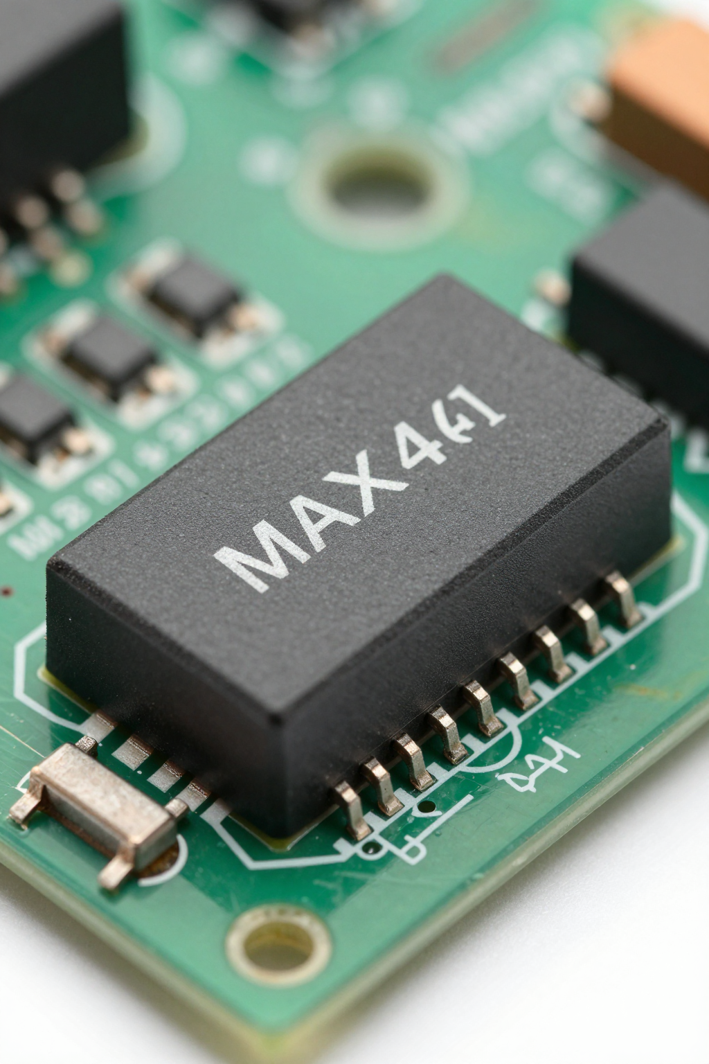
Device description & use-cases
Point: The device is a precision, low-noise, dual rail-to-rail op amp optimized for single-supply systems. Evidence: Its rail-to-rail input/output architecture and low offset/bias metrics suit low-voltage designs. Explanation: Typical roles include sensor conditioning, reference buffering, and low-voltage data-acquisition front-ends where signals sit close to ground or supply rails and accuracy at the ADC input is critical.
Key features at a glance
Point: Quick feature highlighting helps skimmers decide fit. Evidence: Key attributes include rail-to-rail I/O, 2.7 V–5.5 V single-supply range, ~80 µV offset, <1 pA bias, 10 MHz GBW, 5 V/µs slew, ~1 mA quiescent per amp, and SC70/µMAX package options. Explanation: These features optimize low-power precision front ends and buffering in compact footprints.
| Spec | Typical / Note |
|---|---|
| Supply range | 2.7 V – 5.5 V |
| Input offset | ~80 µV (typ) |
| Input bias | <0.3 pA (typ) |
| GBW | ~10 MHz |
| Slew rate | ~5 V/µs |
| Quiescent current | ~1 mA per amp |
Quick Specs & Absolute Ratings (MAX74821ARMZ datasheet highlights)
Electrical summary table (must-have numbers)
Point: A compact electrical summary clarifies design limits. Evidence: Typical conditions: VCC = 5.0 V, TA = 25°C. Key MAX74821 specs include supply voltage range 2.7–5.5 V (max abs 6.0 V), quiescent current ~1 mA/amp, input offset ~80 µV (typ), input bias <1 pA (typ), GBW ≈10 MHz, slew ≈5 V/µs, output swing to within 10–20 mV of rails into 10 kΩ, and common-mode includes rails. Explanation: These numbers distinguish guaranteed vs. typical values; designers should use guaranteed limits for worst-case margining.
| Parameter | Typical | Guaranteed/Notes |
|---|---|---|
| VCC operating | 2.7–5.5 V | Absolute max 6.0 V |
| Quiescent current | ~1 mA/amp | Per amp, TA=25°C |
| Input offset | ~80 µV | Spec sheet lists typ/max |
| Input bias current | <0.3 pA | Typ; watch ta and humidity |
| GBW | 10 MHz | Typ at VCC=5 V |
| Slew rate | 5 V/µs | Typ |
Absolute maximums & thermal limits
Point: Absolute maximum and thermal parameters constrain reliability. Evidence: Absolute ratings include max supply ~6.0 V, input voltages clamped to rails plus limited margin, and junction temperature per package spec; thermal resistance varies by package. Explanation: Follow recommended operating range and apply derating guidance—reduce ambient temp or add thermal vias in high-power environments to maintain junction temps below limits.
Performance Deep-Dive: Noise, Linearity & Frequency Response
Low-noise & DC performance
Point: DC error sources set ultimate precision. Evidence: Typical offset (~80 µV), drift, and pA-class bias current interact with source impedance to create voltage errors. Explanation: For a 10 kΩ source, 0.3 pA bias yields ~3 nV error—negligible; offset and noise density (nV/√Hz) integrated over bandwidth produce ADC input error. Example: at 1 kHz BW with 10 nV/√Hz noise, RMS noise ≈10 nV·√1000 ≈316 nV; compare to ADC LSB to quantify impact.
AC performance: GBW, slew, stability, and compensation
Point: GBW and slew govern closed-loop bandwidth and settling. Evidence: With 10 MHz GBW, a closed-loop gain of 10 yields ~1 MHz small-signal bandwidth; slew (~5 V/µs) limits large-step settling. Explanation: Expect unity or gain-of-1 stability; for capacitive loads, use small series resistors (10–50 Ω). Plotting Bode and step responses for gains of 1 and 10 validates phase margin and slew-limited settling for ADC drive chains.
Design & PCB Layout Guidelines
Power supply decoupling & grounding
Point: Decoupling and grounding prevent oscillation and reduce noise. Evidence: Recommended decoupling is a 0.1 µF ceramic close to VCC pin plus a 1 µF bulk; low ESR ceramics preferred. Explanation: Place caps within 1–2 mm of supply pins, tie grounds to a solid plane, and avoid long traces to decouplers. Verify supply ripple and output stability at the board-level with scope probes.
Input conditioning, feedback network & protection
Point: Input network choices balance noise, offset, and stability. Evidence: Use input resistors that keep Johnson noise low but limit bias-current-induced offset; typical RB ≤10 kΩ for precision. Explanation: For capacitive sources or long lines, add small series resistance and an RC filter (e.g., R=1–10 kΩ, C=10–100 nF) to limit bandwidth. Place feedback components close to the amplifier to minimize stray capacitance; add input clamps or series resistors for ESD resilience.
Typical Applications & Example Circuits
Sensor front-end example (single-supply)
Point: A non-inverting sensor amplifier on a single 5 V rail shows practical performance. Evidence: Example: gain = 5 (Rf=40 kΩ, Rin=10 kΩ) drives ADC; with 80 µV offset and gain 5, offset at ADC ≈400 µV. Explanation: Offset and noise contributions scale with gain; rail-to-rail input/output ensures small signals near ground are preserved without negative supplies, improving dynamic range for low-level sensors.
Low-noise buffer & anti-alias filtering
Point: Use as a buffer before ADC with single-pole or second-order anti-alias filter. Evidence: A unity-gain buffer followed by a 2nd-order Sallen–Key (fc = 100 kHz) provides drive and filtering; GBW supports this topology at modest gains. Explanation: Ensure the buffer's phase margin with the filter topology and keep the ADC sampling aperture and buffer settling time aligned to meet conversion timing.
Testing, Qualification & Procurement Checklist (MAX74821ARMZ datasheet reference)
Bench test procedures to verify key specs
Point: Targeted bench tests validate datasheet claims. Evidence: Measure input offset with low-noise source, bias current via high-value source resistor, noise PSD with spectrum analyzer, GBW with gain-phase analyzer, slew-rate via large-step input, and PSRR/CMRR per datasheet conditions (VCC and TA specified). Explanation: Use VCC=5.0 V and TA≈25°C as baseline; define pass/fail tolerances relative to guaranteed specs and document deviation modes.
BOM, footprint, sourcing & alternate parts
Point: Footprint and sourcing checks prevent rework. Evidence: Verify package land pattern, thermal pad requirements, and ESD handling; confirm date codes and part suffixes on supplier datasheets. Explanation: Before design lock, cross-check the official MAX74821ARMZ datasheet for pinout/land pattern details from the manufacturer reference and include alternate part candidates in the BOM for long-term sourcing resilience.
Key Summary
- Choose this amplifier when low offset (~80 µV), sub-pA bias, and single-supply rail-to-rail I/O are priorities; the MAX74821ARMZ datasheet shows the combination of GBW (~10 MHz) and low quiescent current that suits precision sensor front-ends and ADC drivers.
- Key specs: 2.7–5.5 V supply, ~1 mA quiescent per amp, ~10 MHz GBW, ~5 V/µs slew, and pA-class bias current—use these values for worst-case error budgeting and bandwidth planning.
- Layout and test guidance: tight decoupling, short feedback loops, series resistors for capacitive loads, and bench procedures (offset, bias, noise, GBW, slew) are essential to verify datasheet performance in-system.
FAQ
What does MAX74821ARMZ offer for low-voltage sensor front-ends?
The MAX74821ARMZ delivers rail-to-rail I/O, low offset, and pA-class bias current, enabling accurate amplification of signals near ground on a single 2.7–5.5 V supply. Its modest GBW and low noise make it a strong candidate for precision ADC front-ends when matched to source impedance and bandwidth needs.
How do MAX74821 specs affect ADC selection and error budget?
GBW limits closed-loop bandwidth and thus the anti-alias filter corner; offset and bias current contribute DC error scaled by gain and source impedance; input-referred noise integrated over the system bandwidth defines RMS error. Use these specs to size filters and select ADC LSB to maintain SNR and accuracy targets.
What bench tests should I run before design freeze?
Perform offset and drift, input-bias current via high-value resistor, noise PSD measurement, GBW and phase margin checks, slew-rate and settling time, PSRR/CMRR, and output swing under expected load. Validate under VCC=5.0 V and relevant temperatures; record pass/fail against guaranteed datasheet limits.
Is the MAX74821ARMZ suitable for high-speed data acquisition?
While it has a 10 MHz GBW and 5 V/µs slew rate, it is optimized for precision rather than extreme speed. It suits moderate sampling rates where accuracy and low power consumption are prioritized over ultra-high bandwidth.
Summary
For precision, low-noise, single-supply designs that require rail-to-rail operation, the MAX74821ARMZ datasheet highlights a balanced set of specs—~10 MHz GBW, ~5 V/µs slew, low offset, and pA-class bias—that favor sensor front-ends and ADC buffering. Download and reference the official datasheet from the manufacturer and bench-verify key specs before finalizing the design.