
The official MAX74821 datasheet lists the raw numbers that determine whether this dual rail‑to‑rail op amp suits a design — for example: a 10 MHz gain‑bandwidth product, ~5 V/µs slew rate, input‑offset in the tens of µV, input‑bias in the sub‑pA range, 2.7–5.5 V supply range, and very low quiescent current. This article turns those figures into practical design decisions: which specs drive accuracy, how the pinout maps to common circuits, and step‑by‑step bench tests. The MAX74821 datasheet is referenced conceptually throughout to tie numbers to actions.
Background: What the MAX74821 is and when to choose it (background)
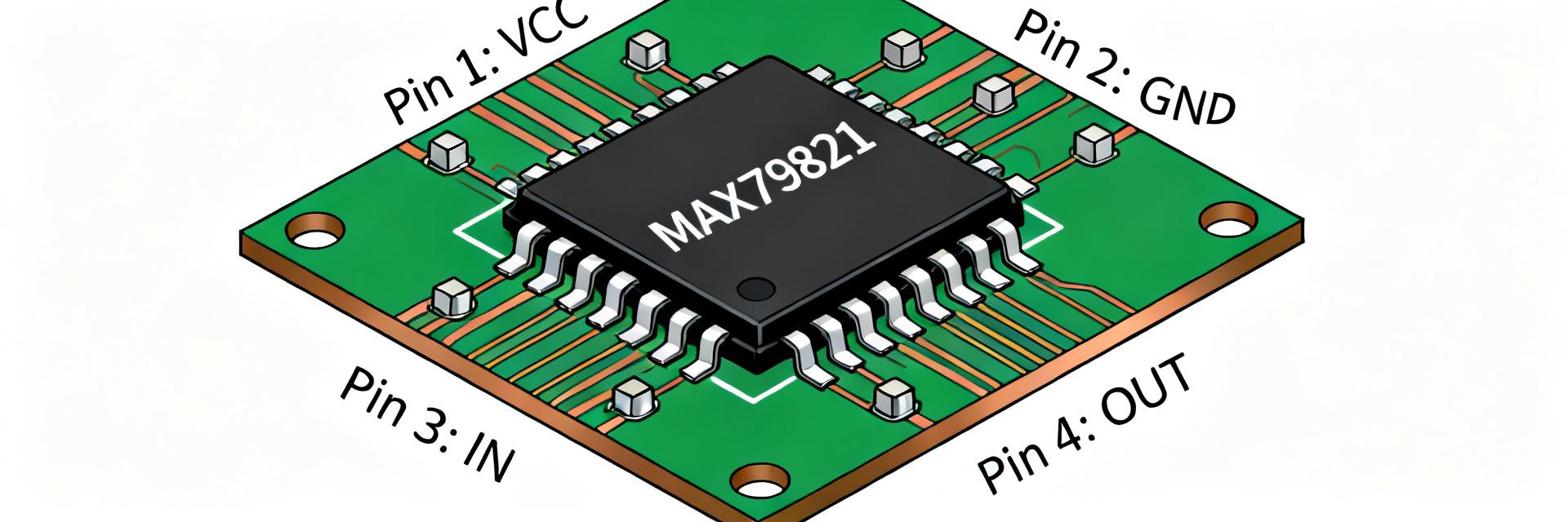
Device overview
Point: The device is a dual‑channel, single‑supply, rail‑to‑rail input/output op amp suited to low‑power precision tasks. Evidence: Top‑line specs include a 10 MHz GBW, ~5 V/µs slew, low input offset (tens of µV), sub‑pA input bias, 2.7–5.5 V supply, and microamp‑class quiescent current. Explanation: Those specs make it a good candidate for precision sensor front ends, portable instrumentation, and battery‑powered signal conditioning where both accuracy and low power matter; the specific part number MAX74821ARMZ‑R7 identifies the package/version used in tight‑space designs.
Key application scenarios
Point: Typical use cases highlight which specs matter. Evidence: For high‑impedance sensor interfaces, offset and bias currents dominate error; for ADC drivers, GBW and slew set settling; for battery systems, supply range and quiescent current determine runtime. Explanation: Short bullets below map cases to the important specs and help choose the device based on measurable design needs.
- Precision bridge or RTD front end — focus on input offset and input‑bias specs to meet µV‑level error budgets.
- Portable ADC driver — GBW and slew rate determine settling time into acquisition windows.
- Low‑power battery instrumentation — supply range (2.7–5.5 V) and quiescent current set standby life.
Pinout & package: pin-by-pin explanation and PCB considerations (case / pinout)
Pin functions and recommended connections
Point: An 8‑pin package exposes the two amplifier channels, power, and ground; correct wiring and decoupling are essential. Evidence: Typical pin assignments for dual op amps are: pin1 OUTA, pin2 −INA, pin3 +INA, pin4 V−/GND, pin5 +INB, pin6 −INB, pin7 OUTB, pin8 V+. Explanation: Use a 0.1 µF ceramic decoupling capacitor placed within 5 mm of V+ to V−, plus a 4.7–10 µF bulk capacitor on the same rail. Keep input and feedback traces short, and avoid routing high‑current returns under sensitive inputs to preserve the specs listed in the datasheet and to maintain stability in closed‑loop configurations.
| Pin | Function | Recommended connection |
|---|---|---|
| 1 | OUT A | Route to feedback network; short trace to decoupled ground |
| 2 | −IN A | Connect to feedback resistor; keep trace short |
| 3 | +IN A | Sensor/ADC input; guard against leakage |
| 4 | V− / GND | Star ground to system return |
| 5 | +IN B | Sensor/ADC input; match routing to channel A |
| 6 | −IN B | Feedback connection for channel B |
| 7 | OUT B | Route to load/buffer; avoid capacitive loads |
| 8 | V+ | Adjacent 0.1 µF decoupling to V−; bulk cap nearby |
Package thermal and board layout tips
Point: Thermal and layout choices affect noise and reliability. Evidence: Small packages typically have modest junction‑to‑ambient thermal resistance; a solid ground plane, thermal vias, and copper pour help. Explanation: Prioritize short feedback traces and a continuous ground plane beneath the op amp to minimize input noise. If driving capacitive loads, add a small series resistor at the output to prevent oscillation. For higher ambient temperatures, derate maximum output current and verify junction temperatures against datasheet thermal limits.
Key electrical specs explained (data analysis)
DC accuracy & input characteristics
Point: Offset, bias, and drift set the DC error floor. Evidence: With input offset ≈ tens of µV and input bias in the sub‑pA range, a 100 kΩ sensor sees negligible voltage from bias current but sees offset directly. Explanation and example: If offset is 20 µV and input bias is 0.5 pA, the error across 100 kΩ from bias is 0.05 µV (50 nV); combined, offset dominates at ~20 µV. Use offset and drift numbers from the specs to build an error budget across temperature and production lot variations.
Dynamic performance: bandwidth, slew, and noise
Point: GBW, slew rate, and noise determine fidelity for transient and AC signals. Evidence: A 10 MHz GBW means unity‑gain bandwidth of 10 MHz; in a gain of 10 configuration expect ~1 MHz closed‑loop bandwidth. A ~5 V/µs slew rate limits how fast large steps settle; output drive and noise density affect ADC SNR. Explanation: For sample‑and‑hold or fast ADC input stages, confirm that closed‑loop bandwidth and slew allow settling to required LSB accuracy. A small table below summarizes key dynamic specs to compare quickly.
| Spec | Typical value | Impact |
|---|---|---|
| GBW | 10 MHz | Sets closed‑loop bandwidth (GBW / gain) |
| Slew rate | ~5 V/µs | Limits large‑signal transient settling |
| Output drive | mA‑class | Defines load and ADC drive capability |
Interpreting datasheet conditions & test limits (data-driven/method)
Typical vs. guaranteed values: what to trust
Point: Typical values show median performance; min/max are guaranteed under specified conditions. Evidence: Datasheet columns for typical and limits include ambient temperature, supply voltage, and load conditions. Explanation: For production margining, design to the worst‑case guaranteed limits at targeted operating temperatures and add safety margins; use typical values only for initial expectation and bench planning.
Measurement conditions to reproduce datasheet numbers
Point: Reproducing datasheet numbers requires matching test conditions exactly. Evidence: Common test conditions include specified VCC (e.g., 5 V), RL to load, ambient temperature, and recommended decoupling. Explanation: Use short ground returns, the same RL as the datasheet, and a low‑noise power supply; any deviation (lower VCC, higher temp, heavier load) will change measured specs, so document differences when validating devices.
Practical bench testing & verification (method / action)
Simple test circuits to validate key specs
Point: Three compact tests validate core specs quickly. Evidence: 1) DC offset: unity follower with low‑noise DVM to measure offset over multiple units. 2) Frequency response: unity and gain=10 sweeps to confirm GBW and phase. 3) Slew/step: apply a fast edge (100–200 mV step) and capture rising slope on scope. Explanation: Expected outcomes: offset near datasheet typical, closed‑loop bandwidth ≈ GBW/gain, slew‑limited slope ≈ specified V/µs. Use scope probe compensation and measurement bandwidth >5× signal bandwidth to avoid loading errors.
Troubleshooting common discrepancies
Point: Measured vs. datasheet mismatches have common causes. Evidence: Typical culprits are poor decoupling, long feedback traces, probe loading, or incorrect test load. Explanation: Checklist — verify decoupling placement, use short ground references, add series output resistor for capacitive loads, check scope bandwidth and probe ground lead inductance, and confirm supply voltage matches test conditions.
Design checklist & quick selection tips (action recommendations)
Quick selection checklist
Point: A concise checklist maps design needs to datasheet lookups. Evidence: Core items are supply range, offset/bias budget, GBW/slew requirement, output drive, package constraints, and temperature range. Explanation: For each item use the MAX74821 datasheet to find guaranteed limits and compare against system requirements; this rapid mapping quickly reveals fit or mismatch for intended application.
When to consider alternatives or supplemental components
Point: The device may need external support in some cases. Evidence: If driving heavy capacitive ADC inputs, consider a series resistor or buffer; if offset must be lower than the native spec, use external trimming or offset cancellation. Explanation: Alternatives or supplements include adding input filtering, using an output buffer for high‑current needs, or selecting a higher‑GBW device for very fast sampling; the pinout and specs guide these choices during schematic review.
Summary
- The MAX74821 datasheet provides the critical specs — supply range, input offset/bias, GBW, slew, and quiescent current — that drive decisions about accuracy, speed, and power in sensor and portable designs.
- Use the provided pinout and PCB tips to place decoupling close to V+ and V−, keep feedback traces short, and add series output resistance when driving capacitive loads to preserve stability and meet the specs.
- Validate key numbers with three bench tests: DC offset, frequency sweep, and slew/step response; reproduce datasheet test conditions to compare results effectively and margin designs for production.
- When tight DC error or faster settling is required, supplement with offset trimming, buffering, or choose a higher‑GBW alternative; the MAX74821ARMZ‑R7 part number denotes the package variant to check when ordering.
FAQ
How do I read the MAX74821 datasheet to verify offset and bias?
Read the DC characteristics table for typical and maximum/minimum columns, note the test conditions (VCC, temperature, RL), and reproduce those conditions on the bench; build an error budget combining offset and bias contributions for your source impedance.
What pinout details in the MAX74821 datasheet matter for PCB layout?
Identify power and ground pins first, place decoupling capacitors within a few millimeters of V+ to V−, keep feedback and input traces short, and use a continuous ground plane; consult the package pin table to avoid crossing sensitive nodes.
Which MAX74821 specs and test circuit should I use to confirm bandwidth and slew?
Use a unity‑gain and a gain=10 frequency sweep to confirm closed‑loop bandwidth (GBW/gain), and a fast step (100–200 mV) captured on a scope with sufficient bandwidth to measure slew rate; compare results to the GBW and slew numbers in the datasheet.
How do I prevent oscillation when driving capacitive loads with MAX74821?
Insert a small isolation series resistor (typically 20 Ω to 50 Ω) directly between the op amp output terminal and the capacitive load, and maintain feedback loop compensation before the resistor to preserve phase margin.





