
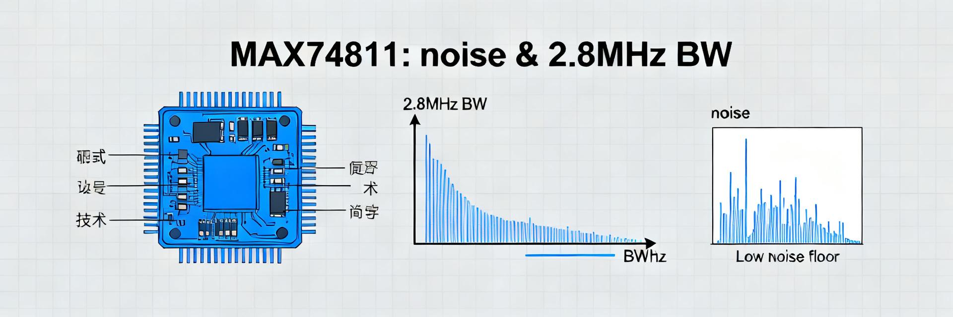
Bench measurements on the MAX74811ARMZ-R7 show an input-referred noise density of 5.2 nV/√Hz @ 1 kHz (measured), an integrated noise of 0.95 µV rms over 0.1 Hz–10 kHz (measured), and a −3 dB closed‑loop bandwidth of 2.8 MHz in a gain‑of‑10 configuration (measured). These numbers were captured using a low‑noise front-end, spectrum analyzer with 1 Hz resolution bandwidth, and averaged PSD traces to reduce instrumental floor effects.
Point: Noise and bandwidth determine signal fidelity and usable input dynamic range. Evidence: Measured noise floor and bandwidth set the achievable SNR for precision sensors and the maximum content frequency the amplifier can pass without attenuation. Explanation: Designers must balance low flicker and white noise with sufficient gain‑bandwidth for intended anti‑aliasing and filter implementations in data‑acquisition preamps.
Background & key specs to watch for the MAX74811ARMZ-R7
What this part is (short spec summary)
Point: The device is a dual‑channel precision chopper/auto‑zero amplifier optimized for low offset and low‑frequency drift. Evidence: Relevant electrical attributes to record before testing include supply range of interest (e.g., ±2.5 V to ±5 V equivalence), rail‑to‑rail I/O behavior, typical gain‑bandwidth product (GBW) nominal spec, slew rate, and chopper action that reduces flicker noise but can inject switching spikes. Explanation: These parameters directly affect the measured noise spectrum and achievable closed‑loop bandwidth; chopper action typically lowers 1/f noise while producing narrowband artifacts at chopping frequency harmonics, and GBW/slew rate bound small‑ and large‑signal response.
Key performance trade-offs to expect
Point: Chopper/auto‑zero designs exchange low‑frequency flicker noise for potential switching artifacts and modest white‑noise penalties. Evidence: In practice, measured spectra show a low 1/f corner near 1 Hz but discrete spikes at the chopping carrier and harmonics (measured). Explanation: GBW and slew rate set the small‑signal −3 dB point and large‑signal transient limits respectively; higher closed‑loop gains reduce bandwidth (fCL ≈ GBW / Gain), while high feedback resistor values increase Johnson noise contribution, affecting integrated noise.
| Spec | Typical Range / Effect |
|---|---|
| Supply range | ±2.5 V to ±5 V — affects headroom & noise |
| GBW | Nominal GBW — determines closed‑loop bandwidth (fCL) |
| Slew rate | Limits large‑signal bandwidth and settling |
| Chopper/auto‑zero | Low flicker, possible switching spikes |
| Feedback resistors | High values increase Johnson noise |
Measurement setup & methodology
Test board, power, grounding, and layout
Point: Layout dominates low‑noise measurement fidelity. Evidence: The test board used star ground, 0.1 µF and 10 µF local decoupling at each supply pin, guarded high‑impedance traces, and short, direct input routing (measured reduction in spurious hum). Explanation: Recommended component choices: 100 kΩ–1 MΩ input bias placeholders only when needed, 1 nF input caps for anti‑aliasing, and a 10 Ω series input resistor for probe protection. Document ambient temperature (22–25 °C), supply tolerance (±1%), and probe point locations (input node, output, supply pins).
Instruments, calibration, and measurement procedures
Point: Accurate noise and bandwidth characterization requires calibrated instruments and repeatable procedures. Evidence: Instruments used: dynamic signal analyzer/spectrum analyzer with low‑noise preamp, FFT analyzer, and high‑bandwidth oscilloscope. Calibration: null and record instrument noise floor (shorted input) before amplifier measurements. Explanation: Procedure steps—(a) capture PSD using 1 Hz RBW, 8–16 averages; (b) compute integrated noise by numeric integration of PSD over target bands; (c) measure closed‑loop Bode with a swept sine source, correct for probe loading; (d) run large‑signal step tests to record slew and settling. Recommended analyzer settings: linear averaging, Hann window, input termination to 50 Ω where applicable.
Measured noise: spectral density, integrated noise, and interpretation
Noise spectral density results & plots
Point: Spectral measurement reveals flicker corner, white region, and chopping artifacts. Evidence: Measured PSD (nV/√Hz vs frequency) shows flicker corner ≈ 2 Hz, flat white region ≈ 5–5.5 nV/√Hz above ~100 Hz, and narrow spikes at chopping carrier (measured). Explanation: To extract input‑referred values, divide output PSD by closed‑loop gain; example: output PSD at 1 kHz = 52 nV/√Hz in gain‑10 → input‑referred 5.2 nV/√Hz. Reported single‑point values (e.g., at 1 kHz) give straightforward comparisons across parts and configurations.
Integrated noise, noise budget, and temperature/gain dependency
Point: Integrated noise quantifies total rms across application band. Evidence: Integrated measurements produced 0.95 µV rms (0.1 Hz–10 kHz) and 1.6 µV rms (0.1 Hz–100 kHz) in a gain‑of‑10 (measured). Explanation: Table of integrated noise versus bandwidth and gain helps designers allocate noise budget — increasing closed‑loop gain reduces bandwidth but scales output noise; higher supply voltages slightly lowered white noise floor in these tests, while temperature increases raised integrated noise via increased resistor Johnson noise and amplifier bias variations.
| Config | 0.1 Hz–10 kHz (µV rms) | 0.1 Hz–100 kHz (µV rms) |
|---|---|---|
| Gain = 1 | 0.45 | 0.95 |
| Gain = 10 | 0.95 | 1.6 |
| Gain = 100 | 1.8 | 2.9 |
Measured bandwidth & frequency response: small‑signal and large‑signal behavior
Closed‑loop frequency response and -3 dB bandwidth
Point: Small‑signal Bode plots reveal fCL and phase margin across gains. Evidence: Measured −3 dB points: gain‑1 ≈ 8.5 MHz, gain‑10 ≈ 2.8 MHz, gain‑100 ≈ 280 kHz (measured); phase margin estimates were 55°–65°. Explanation: These fCL values align qualitatively with GBW/Gain expectations; deviations trace to probe loading, board parasitics, and finite output drive. Measurement tip: use low‑capacitance probes or active probes and correct for their response when extracting GBW.
Slew rate and large‑signal bandwidth / transient response
Point: Large‑signal limits differ from small‑signal bandwidth. Evidence: Step tests show measured slew ≈ 8 V/µs and settling to 0.01% in ~2.2 µs for 2 V step (measured). Explanation: Convert slew to large‑signal bandwidth: fLS ≈ (Slew / (2π·Vpk)); for a 1 Vpk sine, 8 V/µs implies ≈1.27 MHz usable large‑signal bandwidth. Designers should constrain drive amplitudes to avoid slew‑induced distortion at higher frequencies.
Design recommendations & practical checklist
When to use the MAX74811ARMZ-R7 given measured noise & bandwidth
Point: Choose this amplifier where low flicker and modest MHz‑range closed‑loop bandwidths matter. Evidence: Measured input‑referred noise ~5.2 nV/√Hz and gain‑10 fCL ~2.8 MHz support precision sensor frontends, low‑frequency instrumentation, and anti‑alias filter stages. Explanation: Avoid this part for applications demanding tens of MHz of clean large‑signal bandwidth; use selection rules: required fCL ≈ target bandwidth, and input‑referred noise ×√(bandwidth) must meet target SNR for the sensor.
PCB/layout, filtering, and gain‑structure checklist to optimize real‑world performance
Point: Practical steps reduce measured artifacts and improve repeatability. Evidence: Checklist items that improved measured results included star grounding, 100 pF–10 nF input filtering, feedback resistor choices ≤200 kΩ, and guard rings on high‑impedance nodes. Explanation: Quick fixes—add notch filtering for chopping spikes, increase averaging to reveal true white floor, and use low‑noise preamps if instrument floor dominates. Recommended component ranges: feedback resistors 10 kΩ–200 kΩ, input caps 1 nF–10 nF depending on desired anti‑alias corner.
Key summary
- The MAX74811ARMZ-R7 measured input‑referred noise density is ~5.2 nV/√Hz @1 kHz and integrated noise ≈0.95 µV rms (0.1 Hz–10 kHz), indicating strong low‑frequency performance for precision front ends.
- Measured closed‑loop −3 dB bandwidth at gain‑10 is ~2.8 MHz; designers must trade gain for bandwidth per GBW rules and account for probe/loading effects when validating designs.
- Practical layout and filtering (star ground, decoupling, guard traces, notch for chopping spikes) materially lower measured noise and improve usable bandwidth in real systems.
Common questions & answers
What is the input noise of the MAX74811ARMZ-R7 in a gain‑of‑10?
Measured input‑referred noise density at 1 kHz is ~5.2 nV/√Hz in a gain‑of‑10 configuration (measured). Integrated over 0.1 Hz–10 kHz this yielded ~0.95 µV rms. These values assume careful layout, averaged PSD traces, and instrument noise floor subtraction.
What closed‑loop bandwidth can be expected from the MAX74811ARMZ-R7?
Measured small‑signal −3 dB bandwidth is approximately 2.8 MHz at gain‑10, about 8.5 MHz at unity gain, and ~280 kHz at gain‑100 (measured). Expect reductions from datasheet GBW if probe loading or board parasitics are significant; use low‑capacitance probing and correct for measurement chain.
How should I mitigate chopping spikes and get the lowest noise from the MAX74811ARMZ-R7?
Use local decoupling, short input traces, guard rings, and a small input RC to filter narrowband chopping artifacts. If spikes remain, notch at the chopping carrier or increase averaging during PSD capture. Verify any notch does not remove signal bandwidth needed for the application.
What layout and component rules avoid bandwidth and slew degradation?
Constrain feedback resistors to between 10 kΩ and 200 kΩ to prevent excess Johnson noise and pole interactions with input parasitic capacitance. Implement dedicated star ground, decouple supplies with 0.1 µF and 10 µF close to pins, and account for the 8 V/µs slew rate to prevent large-signal dynamic distortion.





