
Background: What the LM318N Is and Where It Fits
What to include
Point: The device is a high‑speed operational amplifier suited for fast amplifier stages and comparator‑like roles where timing matters more than sub‑microvolt precision.
Evidence: Datasheet classifies it in the high‑slew, medium‑bandwidth family commonly used in video buffers and pulse amplifiers.
Explanation: Use this op amp when you need rapid edge handling (high slew) combined with usable small‑signal bandwidth at moderate closed‑loop gains; avoid it for ultra‑low‑noise precision DC references.
Writer guidance
Point: Package choice affects parasitics and thermal limits.
Evidence: Common packages include PDIP and metal can styles with slightly different thermal resistance and lead inductance.
Explanation: Choose PDIP for prototyping convenience; choose metal can or low‑inductance packages for improved high‑frequency stability and thermal performance in production designs. Typical application categories: video buffers, fast integrators, pulse conditioning, and preamplifiers.
Datasheet Snapshot: Pinout & Absolute/Recommended Ratings
Pinout & Pin Functions
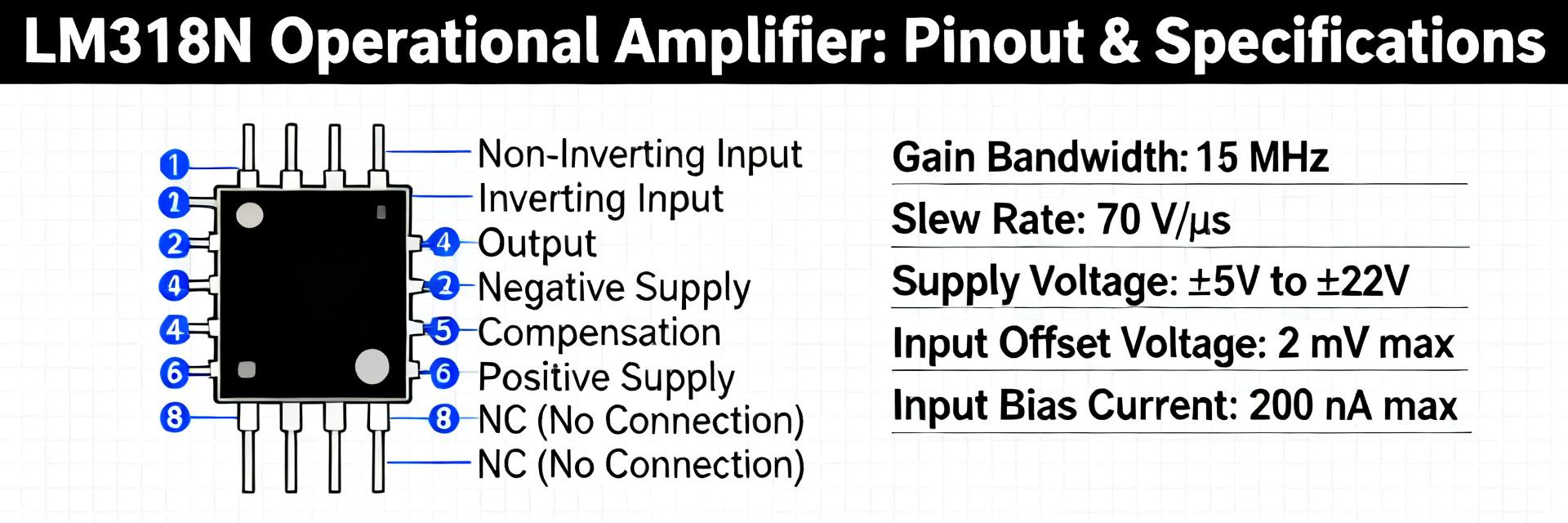
Point: The PDIP pin map assigns inputs, outputs, supplies and compensation/offset pins in a compact arrangement. Evidence: Top‑view PDIP maps show pins for inverting input, non‑inverting input, output, negative and positive supply, and offset null/compensation where present. Explanation: Pay attention to offset null pins and the output pin when routing; keep input traces short and use a solid ground reference to reduce common‑mode induced errors.
| Pin | Name | Function |
|---|---|---|
| 1 | Offset Null | Offset adjust or compensation |
| 2 | Inverting Input | − input |
| 3 | Non‑inverting Input | + input |
| 6 | Output | Signal output |
| 4 | V− | Negative supply |
| 7 | V+ | Positive supply |
Absolute Maximums & Recommended Operating Conditions
Point: Key absolute ratings are supply limits, input differential, and junction temperature. Evidence: The datasheet lists maximum supply rails, allowable input voltage range relative to rails, and thermal junction limits for each package. Explanation: Respecting these limits prevents latch‑up and long‑term drift.
| Parameter | Symbol | Absolute Max | Recommended |
|---|---|---|---|
| Supply voltage | VCC | ±22 V | ±15 V |
| Input differential | VID | ±30 V | within rails |
| Operating temp | TJ | 150°C | −40°C to +85°C |
Performance Metrics Deep‑Dive
Frequency Response & Dynamic Specs
Point: GBW, small‑signal bandwidth and slew rate define both small and large‑signal behavior. Explanation: For a given closed‑loop gain, expected bandwidth ≈ GBW / closed‑loop gain; if step amplitudes require fast edges, ensure slew rate >> required dV/dt = 2π·f·Vpp/2.
DC & Noise Characteristics
Point: Offset, bias currents, input range and noise determine suitability for precision vs. fast‑signal tasks. Explanation: Prioritize offset and drift for DC amplifiers; for video/buffer roles, prioritize slew and bandwidth while managing bias‑induced offsets via input coupling or calibration.
Design & Application Guide
Typical Amplifier Configurations & Compensation
Point: Standard topologies are inverting, non‑inverting and buffer configurations. Explanation: For stability aim for 45–60° phase margin; when closing high gains, compute feedback resistor values so noise gain keeps the amplifier in a stable region. Example: for GBW of 15 MHz and desired BW = 1 MHz, choose closed‑loop gain ≈ 15.
Power Supply Decoupling, Layout & Thermal Tips
Point: Decoupling and PCB layout strongly affect stability and noise. Explanation: Use 0.1 µF ceramic close to each supply pin and a 10 µF bulk nearby. Keep return paths short, ground plane under the device, and add thermal vias for packages with thermal pads.
Example Applications, Common Issues & Quick Fixes
| Circuit | Expected BW | Notes |
|---|---|---|
| Video buffer (f=1 MHz) | ~1 MHz at gain=1 | Check slew for peak edges |
| Fast integrator | BW set by Rf·Cf | Use compensation to avoid peaking |
Troubleshooting Checklist & Recommended Fixes
- Oscillation: Add small series resistors at inputs, increase bypassing, and check probe loading.
- Offset Drift: Correct with offset trim or bias network; check thermal stability.
- Saturation: Ensure sufficient supply headroom and output loading within datasheet drive limits.
Summary
Recap: Focus on pinout clarity for routing, watch the three top performance metrics—GBW, slew rate and offset—and apply disciplined compensation, decoupling and layout practices.
- Clear pin functions and short input routing reduce parasitics and enable expected dynamic performance.
- Match closed‑loop gain to GBW to set bandwidth; ensure slew rate comfortably exceeds required dV/dt for target signals.
- Decouple supplies close to pins, verify thermal path for package, and bench‑measure step response to validate behavior.
FAQ
How should I test slew rate and settling on the bench?
Use a fast step generator into a suitable input network, probe the output with a short ground spring, and capture the edge on an oscilloscope with bandwidth ≥5× the target test frequency. Measure dV/dt for slew and compare to datasheet typical values.
What compensation is needed for stability in closed‑loop designs?
Start with standard inverting/non‑inverting topologies. If peaking occurs, add a small capacitor in parallel with the feedback resistor to shape noise gain and increase phase margin (aim for 45–60°).
How can I reduce output saturation and offset in fast circuits?
Ensure adequate supply headroom, reduce heavy capacitive loads, and employ offset nulling or AC coupling where DC accuracy is less critical. Check thermal stability and biasing.





