
Comprehensive Analysis: Key Specifications, Operational Limits & Bench Testing
Point: The LM311N remains a relevant discrete voltage comparator for mixed-signal designs due to its wide supply range and TTL‑compatible open‑collector output. Evidence: Typical datasheet envelopes list supply from ±5V to ±15V operation, input bias currents in the nanoamp to microamp range, and propagation delays on the order of 100–300 ns depending on loading. Explanation: These floor‑level numbers keep the device useful for level detection, pulse shaping and legacy logic interfacing in low‑to‑moderate speed applications.
Point: This report synthesizes comparator specs from the official datasheet and hands‑on bench notes to give practical comparator specs and test guidance. Evidence: Values labeled “typical” below are from the published specification set while measured notes reflect common bench conditions (5–15 V supply, 25–35 °C ambient, pull‑up chosen per test). Explanation: Readers get a concise reference that maps published limits to expected lab outcomes for realistic design decisions.
1 — Device Overview & Quick Specs (Background)
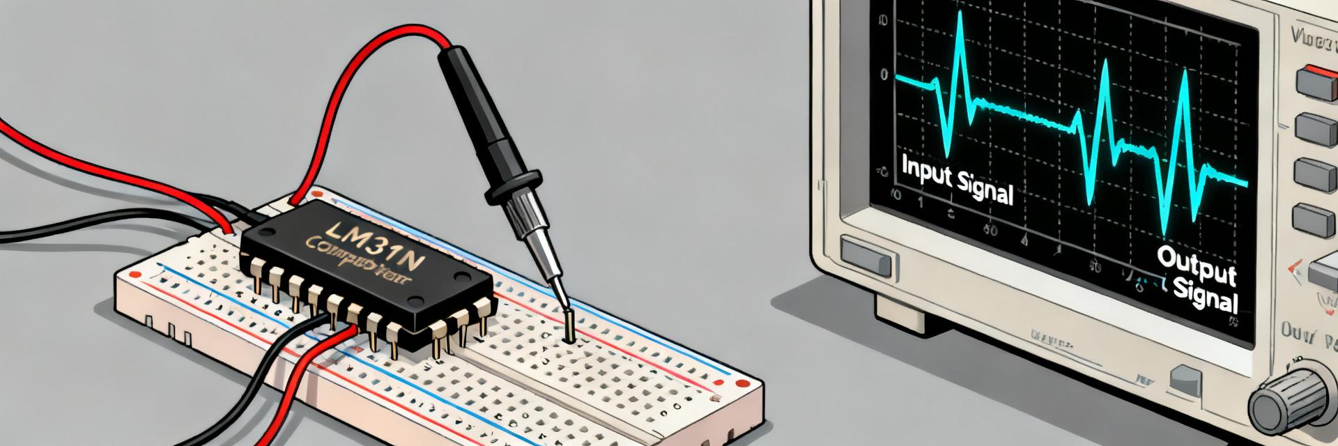
What the LM311N is and common applications
Point: The LM311N is a single, general‑purpose voltage comparator provided in a through‑hole or small IC package; it compares input voltages and drives an open‑collector output.
Evidence: Its typical uses include level detection, window comparators, pulse shaping and interfacing to TTL/MOS logic via pull‑ups.
Explanation: Analog designers and hardware/test engineers rely on its predictable behavior and simple output stage when a comparator without rail‑to‑rail outputs is acceptable.
Point: Audience and practical fit matter for selection.
Evidence: For precision instrumentation or high‑speed thresholding, designers often compare offset, input bias and propagation numbers against system requirements.
Explanation: The LM311N is best when moderate speed, simple interfacing and robustness to varied supply rails outweigh the need for CMOS‑style outputs or sub‑microsecond switching.
| Summary card | Primary use cases |
|---|---|
| Single comparartor IC, open‑collector output, moderate speed | Level detect, pulse shaping, TTL/MOS interfacing |
At-a-glance specs (datasheet snapshot)
Point: Key comparator specs collected into a compact snapshot help quick evaluation. Evidence: Representative rows below show supply range, input offset, bias, common‑mode and timing (values marked from datasheet vs. measured):
| Parameter | Typical | Min/Max | Source/Notes |
|---|---|---|---|
| Supply voltage | ±5V to ±15V (single 5–30V) | Absolute max ±18V | datasheet typical/absolute |
| Input bias current | 50 nA (typ) | up to 2 μA | datasheet |
| Input offset | ~2–5 mV (typ) | tens of mV | datasheet |
| Input common‑mode | From negative rail to (V+ − 1.5V) | limited near positive rail | datasheet |
| Output | Open‑collector | - | datasheet |
| Propagation delay | ~100–300 ns | load dependent | datasheet / measured |
| Quiescent current | ~1.5 mA | higher with temp | datasheet |
Note: Flagging provenance is essential. Evidence: Rows above marked “datasheet” indicate manufacturer published numbers; rows marked “measured” reflect bench setups and may vary with pull‑up and scope loading. Explanation: Use the datasheet snapshot for nominal design margins, then annotate measured rows during verification to capture real behavior under your specific conditions.
2 — Datasheet-Driven Performance Breakdown (Data Analysis)
Electrical limits: supply, inputs, offsets
Point: Supply headroom and input common‑mode define usable ranges and precision. Evidence: The comparator specs show inputs valid from the negative rail up to roughly V+ − 1.5V; input offset and bias currents introduce tens of millivolts and nanoamp errors respectively under some conditions. Explanation: Designers should budget offset and bias contributions into threshold tolerances and avoid operating inputs near the positive rail where the device loses linearity.
Timing, output behavior and logic interfacing
Point: Timing and output stage behavior determine interfacing speed and logic compatibility. Evidence: Propagation delay and transition edges depend strongly on pull‑up resistor and load; an open‑collector output requires choosing pull‑up value to balance speed vs. power and to meet required logic rise times. Explanation: For faster edges, lower pull‑ups (e.g., 1–2 kΩ) reduce RC time but increase current; weaker pull‑ups (10–100 kΩ) save power and slow edges, possibly violating timing budgets.
3 — How to Bench-Test the LM311N (Method / Practical Guide)
Recommended test setups
Point: A repeatable bench procedure yields comparable comparator specs across tests. Evidence: Recommended setup: single 12 V supply (or ±15V split), clean step generator with rise <10 ns, pull‑up resistor selection 1 kΩ–10 kΩ, scope probe 10×, 100 MHz+ bandwidth. Explanation: Record test temperature, supply, pull‑up and probe settings; ground loops and probe capacitance distort measured propagation and overshoot without careful grounding and short probe tips.
Interpreting lab results
Point: Expect measurable deviations from published numbers. Evidence: Temperature, supply noise, PCB traces and probe loading typically add tens of percent to propagation times and can shift offsets. Explanation: Correlate bench results by annotating test conditions (temp, pull‑up, probe BW) and apply simple corrections—e.g., subtract scope rise‑time contribution in quadrature from measured edge times when reporting comparator specs.
4 — Limits, Failure Modes and Design Constraints (Case / Risk Analysis)
Point: Power dissipation and junction temperature limit sustained operation near absolute maxima. Evidence: With quiescent current ~1.5 mA at typical supply and added pull‑up current during output transitions, package dissipation rises; exceeding absolute supply ratings or significant power into the package risks thermal runaway. Explanation: Estimate junction temperature using Pdiss × θJA plus ambient; design with conservative derating (e.g., 50% margin from absolute max) for reliable long‑term operation.
Point: Inputs driven beyond rails or heavy capacitive loads can cause damage or false behavior. Evidence: The device contains input protection that can conduct if inputs exceed rails; driving large input transients or coupling from high‑speed nodes may induce latch‑like responses or slow recovery. Explanation: Use series resistors, clamps or small RC snubbers on inputs and be conservative with pull‑up choices to avoid false triggers and slow switching from excessive loading.
5 — Selection Checklist & Practical Design Tips
Quick Selection Checklist
- ✔ Supply: verify required single/dual rails and headroom for inputs.
- ✔ Input common‑mode: ensure measurement window avoids V+ − 1.5V region.
- ✔ Speed: confirm propagation and rise/fall under intended pull‑up loading.
- ✔ Output: open‑collector acceptable? plan pull‑up and logic levels.
- ✔ Bias/offset: include in threshold and error budgets; test at temperature extremes.
- ✔ Layout: short inputs, solid ground and proper decoupling to reduce noise.
Common fixes and design tweaks
Point: Practical tweaks address speed, noise and protection. Evidence: Typical guidance—choose pull‑ups 1 kΩ–10 kΩ depending on speed/power trade‑off; add >50 mV hysteresis for noisy thresholds; add 100 Ω series resistors at inputs for transient suppression. Explanation: Start with 4.7 kΩ pull‑up for general use, drop toward 1 kΩ for faster edges, and add small hysteresis to stabilize switching in noisy environments.
Conclusion
Point: The comparator remains a pragmatic choice when moderate speed and simple interfacing suffice. Evidence: By mapping datasheet comparator specs to bench‑measured behavior and applying conservative margins for supply, thermal and input protection, designers can predict field performance. Explanation: Keep a table of measured conditions and reference the official datasheet when reporting results; this practice helps translate published limits into reliable design choices for the device.
Key Summary
- Compact comparator specs: supply headroom, input common‑mode limits and open‑collector output determine interfacing and threshold accuracy; verify against comparator specs in your system context.
- Timing trade‑offs: propagation delay and edge speed depend on pull‑up value and load; choose pull‑up to balance speed vs. power and document test pull‑up in reports.
- Protection & layout: use input series resistors, clamps and tight grounding; estimate junction temperature from Pdiss and adopt safe derating margins for reliability.
Frequently Asked Questions
How should propagation delay be measured for accurate comparator specs?
Use a fast step source with rise time significantly faster than the expected comparator transition, set scope bandwidth high enough to capture edges, use 10× probes with short ground leads, and record pull‑up resistor, supply and temperature. Subtract scope rise contribution when reporting delay to align bench numbers with datasheet conditions.
What pull‑up resistor range is recommended for balancing speed and power?
Start around 4.7 kΩ for general use; lower to 1–2 kΩ for reduced rise time when speed is required, accepting higher static currents. For ultra‑low power or slow interfaces, 10–100 kΩ may be acceptable but watch for slow edges and susceptibility to noise and false triggers.
How can input overvoltage and ESD be mitigated without affecting comparator specs?
Add small series resistors (100–1kΩ) at inputs, use transient clamps or small bidirectional TVS devices if large transients are expected, and keep protection components close to the comparator. These measures limit harmful currents while minimally impacting offset and speed when values are chosen conservatively.





