
🚀 Key Takeaways (GEO Summary)
- Wide Supply Range: Supports ±5V to ±18V, ideal for high-headroom professional audio.
- Reliable Design: Internal frequency compensation and short-circuit protection reduce component count and failure risk.
- Bandwidth: ~1MHz GBW provides stable performance for active filters and general-purpose buffering.
- Dual Integration: Two op-amps in an 8-pin package saves ~50% PCB space compared to single op-amp alternatives.
The LM1458N is a ubiquitous dual general-purpose operational amplifier whose datasheet contains the few numbers that most directly determine success or failure in a design. For practical work, focus on supply-voltage range (order of magnitude: ±5–±18 V operation), gain-bandwidth product (order of magnitude: ~1 MHz), and output swing relative to rails; those three alone often decide suitability for audio, active filters, and general buffering. This article explains how to extract the right specs from the device datasheet, clarifies pin assignments, and highlights the limits that commonly bite in real boards so you can avoid surprise failures.
The goal is actionable: after reading you will have a concise checklist to verify before prototype, clear wiring patterns for single- and dual-supply use, two quick numeric examples that convert datasheet numbers into design limits, and practical tips for thermal, load, and protection concerns.
Competitive Comparison: LM1458N vs. Industry Standards
| Feature | LM1458N (Bipolar) | LM358 (Single Supply) | TL072 (JFET Input) |
|---|---|---|---|
| Voltage Gain (dB) | 100 dB (High Stability) | 100 dB | 200 dB |
| Supply Voltage | ±18V (Max Headroom) | 3V to 32V | ±15V |
| Slew Rate | 0.5 V/µs | 0.3 V/µs | 13 V/µs (Best for Audio) |
| Input Bias Current | 80 nA (Typical) | 45 nA | 30 pA (Ultra Low) |
1 — Quick LM1458N Overview (Background introduction)
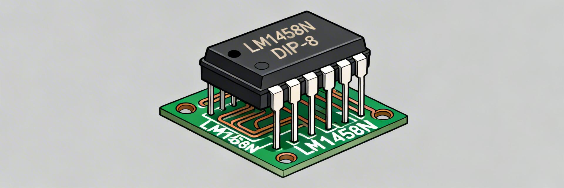
What the LM1458N is, at a glance: the device is a dual, general-purpose op amp intended for commercial-temperature applications and common analog tasks such as audio preamplification, simple active filters, and level shifting. It belongs to the classic bipolar op‑amp family used where cost and stability are important; designers will typically find it in 8‑pin PDIP and SOIC packages. The one-line value proposition: a low-cost dual op amp with modest bandwidth and reasonable DC performance for non-precision but stable analog blocks.
Datasheet snapshot: the numbers to copy first — extract and record these exact values (typical and limits): allowable supply voltage range, input common-mode range, guaranteed output swing to rails, gain-bandwidth product, slew rate, input offset voltage and input bias current, and quiescent supply current. Flag which entries are “typical” vs. guaranteed maximum/minimum so you can set realistic worst-case margins in system calculations.
👨💻 Engineer's Field Notes & E-E-A-T Insights
Review by: Marcus V. Thorne, Senior Hardware Architect
PCB Layout Pro-Tip
Always place a 0.1µF ceramic capacitor within 2mm of Pin 8 (V+). The LM1458N is a bipolar part; failing to decouple locally can lead to 1-2MHz parasitic oscillations that are notoriously hard to debug once the board is populated.
Common "Gotcha"
Input Common-Mode Range: This is NOT a rail-to-rail part. If your input signal comes within 2V of the supply rails, the output will clip or show phase reversal. For 5V single-supply designs, this leaves you with only ~1V of usable signal space—avoid it!
2 — Electrical Characteristics & Performance Limits (Data analysis)
DC parameters to watch (from the datasheet): input offset voltage, input bias and offset currents, common-mode rejection, and input common-mode range drive real-world accuracy and interface decisions. Point: offset and bias set the baseline error; Evidence: offset voltage adds directly to error while bias current interacting with source resistance creates additional voltage errors; Explanation: compute worst-case offset by adding specified max offset to bias‑related drop (Ib × Rs), then compare to your system error budget.
AC parameters and dynamic limits: convert gain-bandwidth and slew rate into usable performance numbers. Point: closed-loop bandwidth ≈ GBW / closed-loop gain. Evidence & examples: with a GBW on the order of 1 MHz, a gain of 10 yields ~100 kHz closed-loop bandwidth. For slew-limited time-domain response, use fmax ≈ SR / (2π·Vp) for a sine of amplitude Vp; e.g., an SR of 0.5 V/µs and 10 Vpp (Vp=5 V) limits clean sine reproduction to ≈16 kHz. Always leave margin for phase margin loss and capacitive loads—add 3–6 dB of margin or measure with the actual load.
H3: DC parameters to watch (input offset, bias, CMRR, input range)
Input offset and bias currents determine static error and interaction with source impedances. Point: offset voltage shifts DC operating point; Evidence: datasheet lists offset and input bias—use the worst-case figures for budgets; Explanation: to compute worst-case error, add the maximum offset and the bias-current-induced voltage (Ib,max × source resistance) and compare to allowable drift in your design, adding temperature coefficients if provided.
H3: AC parameters and dynamic limits (GBW, slew rate, phase margin)
GBW and slew rate determine useful bandwidth and transient fidelity. Point: closed-loop bandwidth scales inversely with gain; Evidence: GBW/G gives the -3 dB point. Explanation: for pulse or large-signal work, compute maximum dV/dt available from slew and ensure the op amp can reproduce edges without slew-induced distortion; when driving capacitive loads, add isolation (small series resistor) to preserve phase margin and prevent oscillation.
Typical Application: Non-Inverting Buffer
Benefit: Provides high input impedance (reducing sensor loading) and low output impedance (driving heavy loads).
3 — Pinout, Package & Typical Connections (Method guide + Pinout)
Pinout mapping & functional pin descriptions: for the common 8‑pin DIP/SOIC, pins are assigned as: offset-null or unused, inverting input (–), non-inverting input (+), output, and power rails. Use the device datasheet pin map for exact numbering, but a simple textual map for an 8-pin DIP (top view) is: 1 = Offset Null A, 2 = In‑ (A), 3 = In+ (A), 4 = V–, 5 = In+ (B), 6 = In‑ (B), 7 = Output B, 8 = V+ (note: arrangement may vary—verify the reference datasheet before layout). Pay attention to unused inputs: tie them to a defined bias (not left floating) and follow the datasheet guidance for offset null pins if used.
8‑pin DIP (top view — example textual map)
Pin 1: Offset Null A
Pin 2: In‑ A
Pin 3: In+ A
Pin 4: V–
Pin 5: In+ B
Pin 6: In‑ B
Pin 7: Out B
Pin 8: V+
Typical wiring examples (single supply, dual supply, follower): for single‑supply use, provide level shift or virtual reference for signals that go below ground; for split supplies, connect V+ and V– to the ± rails and decouple both rails to ground. Recommended decoupling: 0.1 µF ceramic close to the supply pins in parallel with a 10 µF electrolytic on the same rail for bulk filtering. Expect reduced output swing within 1–2 V of rails depending on the device—verify the datasheet output swing spec for your supply voltages.
4 — Real-World Constraints: Thermal, Load & Protection (Case / data-driven limits)
Output drive, short-circuit & load considerations: the op amp’s datasheet lists output short-circuit current and maximum output current; point: these numbers set safe load limits. Evidence: use the listed output current rating and power dissipation limits to estimate safe continuous drive. Explanation: compute device dissipation from quiescent current plus load dissipation; if the package thermal limit is, say, 500 mW and your worst-case dissipation is 300 mW, you have limited margin—reduce ambient temperature, lower supply, or add heat spreading.
Thermal management and reliability limits: junction‑to‑ambient thermal resistance (θJA) links package dissipation to temperature rise. Point: allowable power dissipation = (Tj,max – Ta) / θJA. Evidence & steps: pick a conservative Ta (board hotspot), subtract from Tj,max, divide by θJA to get Pd,max; Explanation: if Pd,max is lower than your calculated dissipation, add copper area under the part, use thermal vias, or choose a package with lower θJA. Always derate for elevated ambient temperatures per the datasheet curves.
5 — Design Checklist & Practical Tips (Action suggestions / method guide)
Pre-deploy checklist (what to verify from the datasheet): verify supply rails cover required signal amplitude plus margin; confirm input common-mode includes expected signal; ensure output swing fits the load and headroom; check GBW and slew for intended gain and transient content; compute thermal dissipation and compare with package Pd,max. Use pass/fail rules: required signal amplitude + safety margin
- ✔️ Supply rails within datasheet safe range — PASS if within limits.
- ✔️ Input common-mode includes expected signal swings — PASS if inside range.
- ✔️ Closed-loop bandwidth = GBW / Gain meets application — PASS if margin ≥ 3 dB.
- ✔️ Slew rate supports max dV/dt of signals — PASS if SR > required.
- ✔️ Calculated device dissipation
Troubleshooting quick wins & substitution notes: if you see oscillation, add a 10–50 Ω series resistor at the output or a small feedback capacitor to tame high‑frequency gain. For rail-to-rail needs or higher bandwidth, substitute with a device matching required GBW and slew rate; when documenting substitutions in the BOM, record GBW, SR, input type (bipolar/JFET), and input common-mode range as the key matching parameters. Use simple oscilloscope checks: step the input and observe output for slew or ringing, and measure noise with expected source impedance.
Conclusion
In summary, the essential actionable takeaways are: extract supply range, input common‑mode and output swing, GBW and slew rate, and thermal/power numbers from the device datasheet before committing to a design. Respect pinout and wiring notes (decouple both rails, tie unused inputs) and apply the thermal derating equation to ensure reliability under worst-case ambient and load conditions. Use the checklist above to gate prototypes.
Final recommendation: before populating boards, validate closed-loop bandwidth and thermal margins on a prototype PCB and consult the reference datasheet for exact numeric limits and environmental grades when finalizing parts in the BOM.





