
Key Takeaways
- High Precision Sensing: Tera-ohm input impedance ($10^{12} \Omega$) eliminates signal loss when using high-impedance sensors.
- Superior Signal Clarity: 12 V/µs slew rate prevents distortion in high-speed audio and pulse applications.
- Minimal DC Error: Ultra-low 30pA input bias current ensures accuracy in long-term integrators and buffers.
- Fast Settling: Reaches 0.01% accuracy in just 1.5µs, ideal for rapid data acquisition front-ends.
The LF356N is a classic J‑FET input operational amplifier often compared by designers across bandwidth, slew rate, input noise, input bias/offset, and allowable supply range. Small differences in these metrics shift suitability between filters, unity buffers, and precision amplifiers. This digest aims to deliver a compact, testable summary of the LF356N datasheet and practical performance takeaways for rapid selection and bench verification.
Comparative Analysis: LF356N vs. Industry Standards
| Parameter | LF356N (JFET) | TL071 (Standard) | Design Benefit |
|---|---|---|---|
| Slew Rate | 12 V/µs | 13 V/µs | Crisp pulse response; low THD |
| Input Bias Current | 30 pA (typ) | 65 pA (typ) | Reduced DC offset in high-R circuits |
| Settling Time (0.01%) | 1.5 µs | 2.0 µs | Faster response in multiplexed inputs |
| Input Impedance | $10^{12} \Omega$ | $10^{12} \Omega$ | Zero loading on delicate sensors |
What the LF356N Is and Where it's Used (background)
J‑FET input architecture: practical implications
Point: The J‑FET input stage gives very high input impedance and low input bias currents compared with bipolar input amps, which changes how designers bias and protect inputs. Evidence: Typical datasheet bias currents sit in the low nanoamp range, while input resistance is often megaohms to gigaohms. Explanation: High input impedance reduces sensor loading and permits simple RC input networks, but the designer must consider input protection for large differential or ESD events and bias paths for DC stability.
Point: Offset behavior and noise differ versus bipolar designs. Evidence: J‑FET inputs often show larger voltage noise at low frequencies but lower current noise. Explanation: For voltage‑sensitive applications (audio buffering, active filters) the J‑FET tradeoff favors minimal sensor loading; for the lowest voltage noise in precision DC amplifiers, alternate input types may be preferable. The datasheet provides the specific offset and noise figures to guide that choice.
💡 Engineer's Insight: Bench Optimization
"When working with the LF356N, always beware of 'Phase Reversal.' If the input common-mode voltage drops below the negative supply rail, the output can swing to the positive rail unexpectedly. To prevent this, ensure your input signals remain at least 3V above the V- rail. Also, prioritize tight PCB layout: a 0.1µF ceramic capacitor placed within 3mm of the V+ pin is non-negotiable for high-speed stability."
— Marcus V. Thorne, Senior Analog Applications Engineer
Typical application domains and form factors
Point: Common uses include active low‑pass/high‑pass filters, instrumentation front‑ends, audio buffering, integrators, and general analog signal conditioning. Evidence: Package choices are standard through‑hole and surface‑mount DIP and SOIC variants with familiar pinouts for single op amp integration. Explanation: Designers pick the LF356N when input impedance and moderate bandwidth are prioritized over ultra‑low voltage noise or rail‑to‑rail output swing.
*Hand-drawn schematic, non-precise schematic representation (手绘示意,非精确原理图)
Typical Application: Unity Gain Buffer
The LF356N excels as a buffer for high-impedance sensors. By connecting the output directly to the inverting input, you create a high-precision voltage follower that prevents the measurement tool from 'sucking' current out of your signal source.
Key Specs at a Glance (data analysis)
Electrical headline specs to read first
Point: Scan supply voltage range, input offset and drift, input bias current, input impedance, open‑loop gain, unity‑gain bandwidth, slew rate, output drive/swing, and quiescent current as the primary checklist. Evidence: The datasheet lists each under typical and absolute maximum conditions. Explanation: For example, a 10‑nA input bias implies that with a 1‑MΩ source the DC error can be ~10 mV unless bias compensation or buffering is used; a 3 V/µs slew rate bounds fastest clean step responses and limits large‑signal bandwidth in high‑gain stages.
- ✅ Supply Range: ±5V to ±18V (Dual supply recommended for maximum linear range).
- ✅ Input Offset: 3mV (typ) – ensure trimming is available for DC-accurate tasks.
- ✅ Open-Loop Gain: 106 dB – provides high loop gain for precision filter feedback.
Performance Summary: What to Expect on the Bench
Frequency response, gain‑bandwidth limits and compensation
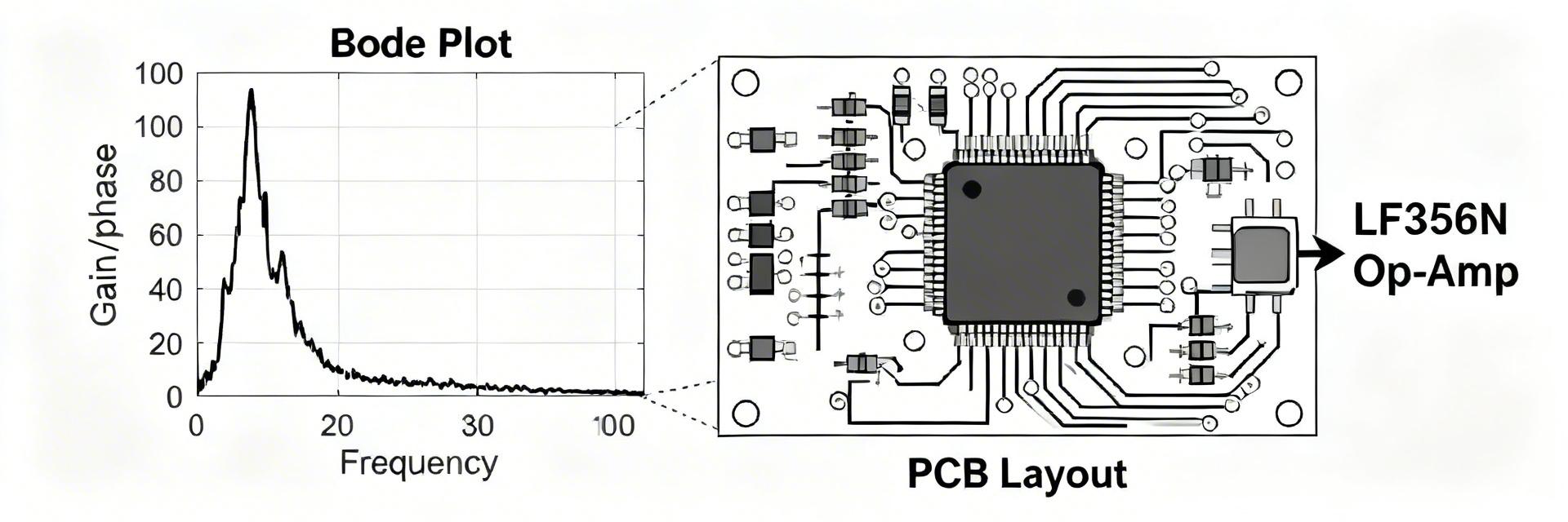
Point: Expect the small‑signal frequency response to follow the unity‑gain bandwidth and closed‑loop gain product; compensation alters phase margin. Evidence: Datasheet GBW and open‑loop rolloff set the initial prediction for closed‑loop bandwidth. Explanation: Run Bode plots at unity gain and at target gains; if you see peaking near the crossover, add a small feedback capacitor across the feedback resistor or increase closed‑loop gain to restore phase margin.
Design & Application Guidelines
Powering, decoupling, layout and thermal notes
Point: Proper decoupling and layout preserve stability and low noise. Evidence: Datasheet reliability/thermal sections show derating and quiescent dissipation that limit continuous ambient temperature. Explanation: Place 0.1‑µF ceramic decouplers close to the supply pins and a 10‑µF bulk cap nearby. Keep input traces short, separate sensitive nodes from digital switching, and provide a solid analog ground plane.
Quick Troubleshooting Checklist
- Oscillations? Check for capacitive loading on the output. Add a 50Ω isolation resistor.
- Excessive Drift? Check for thermal gradients across the PCB. Keep away from power transistors.
- Output Clipping? Verify supply rails; the LF356N is NOT rail-to-rail. Expect ~2V headroom loss.
Summary
The LF356N serves well where a J‑FET input, high input impedance, and moderate bandwidth are primary requirements; consult the datasheet headline specs (input bias/impedance, GBW, slew, offset, and supply range) to confirm suitability, then validate on the bench with the provided checklists.





