
Designing robust current-sensing circuits for electric vehicles (EVs) and hybrid systems often hits a wall when common-mode voltage spikes meet strict automotive reliability standards. You frequently struggle to balance precision, noise immunity, and AEC-Q100 compliance in high-voltage environments. The INA241B3EDRQ1 emerges as a critical solution, offering enhanced PWM rejection and bidirectional sensing capabilities tailored specifically for these demanding applications. This guide breaks down the essential key specs and automotive compliance requirements needed to integrate this component successfully into next-generation powertrain and battery management systems.
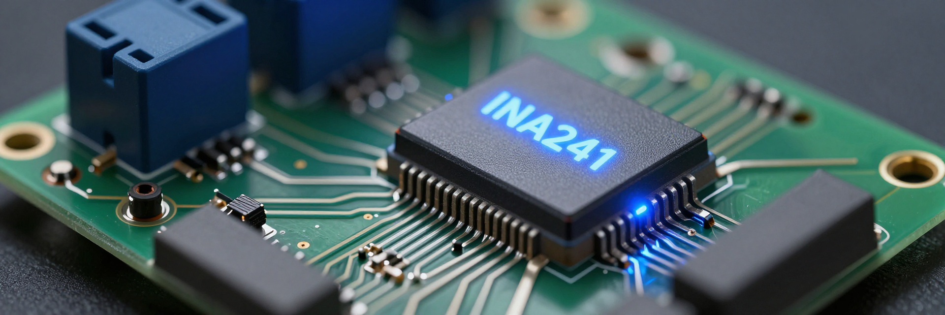
Understanding the Core Architecture of INA241B3EDRQ1
Bidirectional Sensing and Common-Mode Voltage Range
You need a device that operates reliably across wide voltage swings. The INA241B3EDRQ1 senses current across shunt resistors with common-mode voltages ranging from -4 V to 80 V. This extensive range is vital for monitoring high-voltage battery packs where potential differences fluctuate significantly during operation. Its bidirectional output capability allows you to monitor both charging and discharging currents seamlessly. This feature eliminates the need for complex switching logic or multiple sensor setups, simplifying your Battery Management System (BMS) architecture while maintaining data integrity during regenerative braking cycles.
Enhanced PWM Rejection Mechanism
Standard amplifiers often fail in motor control applications due to large differential voltages caused by fast-switching inverters. You face significant measurement errors if external filters are not perfectly tuned. The INA241B3EDRQ1 utilizes a proprietary filtering technique designed to reject these PWM-induced artifacts effectively. This internal mechanism ensures stable readings without requiring bulky external components. By mitigating noise at the source, you achieve higher signal fidelity in traction inverters, ensuring precise torque control and improved efficiency in EV drivetrains.
Critical Key Specs for High-Precision Design
| Parameter | Typical Value | Unit | Impact on Design |
|---|---|---|---|
| Input Offset Voltage | ±5 | µV | Determines low-current accuracy floor |
| Common-Mode Range | -4 to 80 | V | Enables high-side sensing in HV buses |
| Bandwidth | 100 | kHz | Affects transient response speed |
| Temperature Drift | 0.05 | µV/°C | Critical for calibration stability over temp |
Offset Voltage and Gain Accuracy Analysis
Precision defines the success of your current loop. The typical input offset voltage of ±5 µV directly impacts low-current measurement accuracy, which is crucial for detecting standby states or small leakage currents. You must also consider gain error tolerance and temperature drift coefficients. These parameters determine how well your system maintains calibration stability over varying thermal conditions. Proper understanding of these specs allows you to design compensation algorithms that mitigate drift, ensuring consistent performance throughout the vehicle's operational life.
Bandwidth and Slew Rate Performance
Signal fidelity during rapid transient events depends heavily on bandwidth characteristics. You should evaluate how the amplifier’s slew rate affects response times in dynamic load scenarios. Selecting appropriate shunt resistor values is a trade-off between resolution and speed. Lower resistance reduces power loss but may compromise signal-to-noise ratio, while higher resistance improves resolution but increases heat dissipation. Optimizing this balance ensures you capture fast-changing current profiles accurately without introducing latency in safety-critical protection circuits.
Navigating Automotive Compliance Standards
AEC-Q100 Qualification and Temperature Grades
Automotive Compliance is non-negotiable for production vehicles. The INA241B3EDRQ1 adheres to AEC-Q100 Grade 1 specifications, operating reliably from -40°C to +125°C ambient temperature. You benefit from rigorous testing protocols, including thermal cycling and mechanical stress tests, which validate durability under harsh conditions. This qualification assures you that the component can withstand the vibrations, humidity, and extreme temperatures found in engine bays and chassis-mounted modules, reducing field failure rates and warranty costs.
Functional Safety Integration Considerations
Integrating this component into safety-critical systems requires adherence to ISO 26262 guidelines. You must perform failure mode analysis to understand potential diagnostic coverage gaps. Implementing redundant sensing paths or cross-checking mechanisms enhances overall system reliability. By leveraging the device’s predictable behavior and documented fault modes, you can develop robust software routines that detect anomalies early. This approach supports ASIL-rated designs, ensuring that current sensing contributes positively to the functional safety concept of your EV platform.
Practical Implementation Strategies for EV Systems
Layout Guidelines for Noise Immunity
PCB layout plays a pivotal role in achieving specified performance. You should minimize ground loops and parasitic inductance near the sense inputs to prevent noise coupling. Place decoupling capacitors close to the power pins and utilize star-grounding techniques to maintain reference stability. Poor layout practices can negate the benefits of high-quality silicon, leading to erratic readings. Careful attention to trace width, layer stack-up, and return paths ensures accurate measurements even in noisy electromagnetic environments typical of automotive electronics.
Interfacing with Microcontrollers and ADCs
Matching the amplifier’s output impedance with downstream Analog-to-Digital Converters (ADCs) is essential for signal integrity. You need to account for settling time and sampling rates to avoid aliasing effects. When integrating with smart sensor hubs or isolated interfaces, ensure digital communication lines are shielded appropriately. Proper buffering and filtering at the interface stage preserve the analog quality of the sensed current, enabling precise control algorithms to function correctly within the microcontroller environment.
Key Summary
- The INA241B3EDRQ1 offers -4 V to 80 V common-mode range for versatile EV battery monitoring.
- Enhanced PWM rejection technology ensures accurate current sensing in noisy inverter environments.
- AEC-Q100 Grade 1 compliance guarantees reliability across -40°C to +125°C temperature extremes.
- Low offset voltage and precise gain specs support high-fidelity low-current measurements.
- Optimal PCB layout and ADC interfacing strategies are critical for maximizing performance.
Frequently Asked Questions
Why is the INA241B3EDRQ1 preferred for EV inverters?
You prefer this model because its enhanced PWM rejection capability handles the high-frequency noise generated by fast-switching IGBTs or MOSFETs in inverters. Unlike standard amplifiers, it provides stable readings without complex external filtering, simplifying design and improving reliability in traction control applications.
What does AEC-Q100 Grade 1 mean for this component?
AEC-Q100 Grade 1 indicates that the device has passed rigorous automotive qualification tests for operation between -40°C and +125°C. You can trust its durability against thermal cycling, vibration, and humidity, making it suitable for harsh under-hood or chassis-mounted environments in modern vehicles.
How do I choose the right shunt resistor value?
You must balance power dissipation with signal resolution. A lower resistance minimizes heat but reduces voltage drop, potentially affecting SNR. Calculate the expected peak current and select a resistor that keeps the voltage drop within the amplifier’s linear range while maintaining sufficient headroom for accurate low-current detection.
Can the INA241B3EDRQ1 handle negative common-mode voltages?
Yes, the INA241B3EDRQ1 supports a wide common-mode voltage range from -4 V to 80 V. This allows for bidirectional current sensing, which is essential for monitoring both charging and discharging phases in battery management systems and regenerative braking cycles.