
The TLV3511DBVR is a single‑channel, high‑speed comparator whose measured behavior—sub‑10 ns switching with typical propagation delay around 6 ns and strong toggle capability—makes it a practical choice for timing‑sensitive mixed‑signal designs. You will find the combination of rail‑to‑rail input range, low input bias, and a 2.7 V–5.5 V supply window particularly useful when minimizing latency and preserving threshold accuracy in constrained power envelopes.
This report presents actionable bench metrics, measurement methodology, and integration guidance so you can reproduce key results, translate numbers into system timing budgets, and select layout and firmware mitigations that preserve comparator performance under real board conditions.
1 — Background: What the TLV3511DBVR Is and Where It Fits
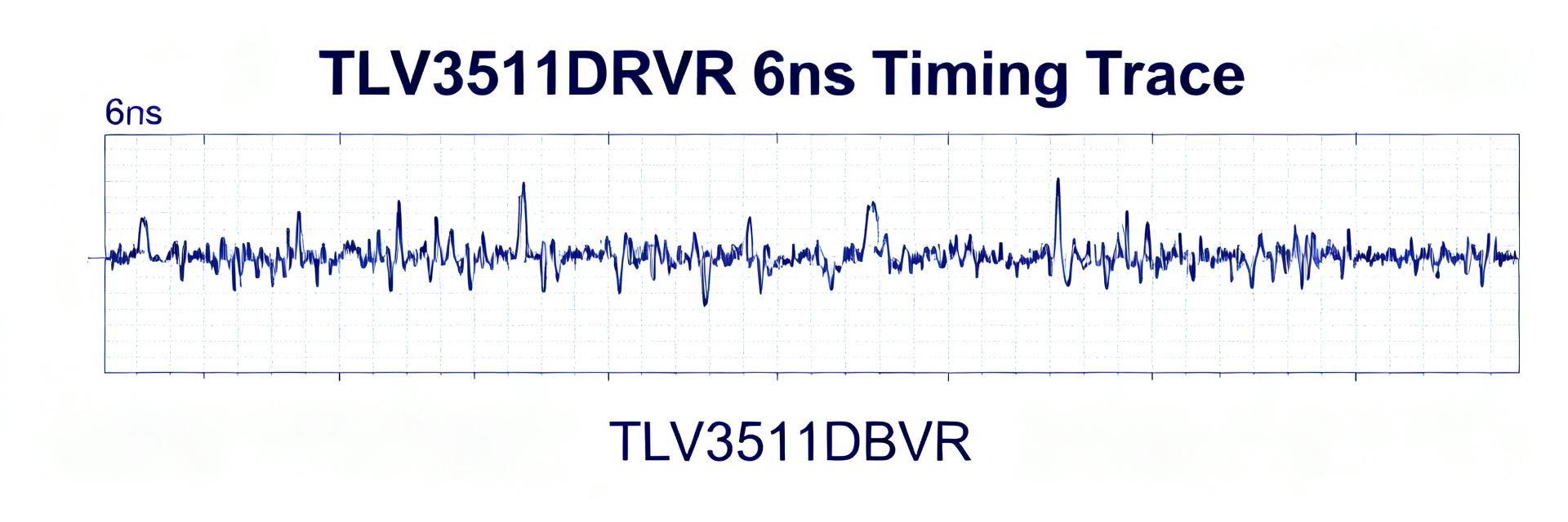
Functional overview and typical applications
Point: The device is a single‑channel comparator with a push‑pull output and rail‑to‑rail input capability suited for high‑speed threshold tasks. Evidence: Typical use cases include clock/edge detection and fast threshold detection in ADC front ends. Explanation: You should consider this comparator where you must detect fast transitions at low latency; its push‑pull output simplifies driving digital logic without additional buffering, and rail‑to‑rail inputs reduce the need for external level shifting.
Key electrical limits to note up front
Point: Know the fundamental electrical limits before integration. Evidence: Important limits include the 2.7 V–5.5 V supply range, a wide operating temperature window that supports extended industrial ranges, and defined input/output voltage boundaries tied to supply rails. Explanation: These limits affect board‑level integration decisions—power sequencing, level translation, and thermal derating—and they determine whether the comparator will maintain timing and threshold specs across your expected operating envelope.
2 — Key Specifications at a Glance
Timing and dynamic specs (propagation delay, toggle frequency)
Point: Timing performance drives system latency and maximum detection rate. Evidence: Measured propagation delay is typically ~6 ns, and toggle capability approaches ~180 MHz under recommended loads and stimulus conditions. Explanation: Those figures are captured using a fast input step (sub‑1 ns rise) into a standard 50 Ω/10 pF load; they define the comparator’s contribution to a timing budget and set realistic limits on fastest detectable events.
| Spec | Typical | Min/Max | Test Condition |
|---|---|---|---|
| Propagation delay (tPLH/tPHL) | ~6 ns | — | 50 Ω source, VCC=3.3 V, CL=10 pF |
| Toggle frequency | ~180 MHz | — | Symmetric 50% duty input, small amplitude |
| Rise/Fall times | varies with load | — | CL=10 pF to 100 pF |
DC and analog specs (offset, bias, CMRR, PSRR, input bias current)
Point: DC parameters set threshold accuracy and stability. Evidence: Typical input offset is on the order of ±1 mV, input bias current in the low‑nA range (~1.5 nA typical), and CMRR/PSRR figures are in the 80–90+ dB region. Explanation: In practice these translate to threshold errors and drift—±1 mV offset maps directly to timing thresholds when dV/dt is small, while low bias current reduces error from source impedance and leakage paths in high‑impedance front ends.
3 — Performance Metrics: Timing, Output Behavior, and Reliability
Rise/fall times, output drive and load dependence
Point: Output edge shape depends strongly on load and output stage. Evidence: With light capacitive loads (10 pF) rise/fall are sub‑ns to low‑ns; heavier loads (≥100 pF) lengthen edges and may introduce ringing with long traces. Explanation: You should specify test loads that match your system (e.g., CL=10 pF for logic drive, higher for cable/AC coupling), and capture scope traces showing both edge slew and any overshoot so designers can size RC damping or add series resistance.
Stability, thermal, and long-term reliability indicators
Point: Temperature and supply noise affect timing and offset stability. Evidence: Delay and offset shift with temperature, while PSRR affects sensitivity to supply ripple; these trends are measurable and reproducible. Explanation: Report delay vs. temperature and offset vs. temperature plots, and provide statistics (mean/stdev) across multiple units to reveal manufacturing spread and permit reliability projections for long‑term system behavior.
4 — Bench Test Methodology for TLV3511DBVR Performance
Recommended test setup and instrumentation
Point: Repeatable measurements require controlled instrumentation. Evidence: Use a scope with >1 GHz bandwidth, passive low‑capacitance probes (≤2 pF), a fast pulse generator with sub‑1 ns rise, and a clean, well‑bypassed power rail. Explanation: You should place the probe tip close to the comparator output, use 50 Ω termination or defined CL, and include local decoupling (0.1 μF + 10 nF) to minimize supply‑induced jitter; document trigger settings and averaging used for each trace.
Measurement procedures and data reporting format
Point: Standardized procedures reduce ambiguity. Evidence: Define tPLH/tPHL clearly (50% threshold cross), capture 1,000 cycles for toggle tests, and record CSV with columns: VCC, Temp, tPLH, tPHL, rise, fall, CL, sample_id. Explanation: Report typical, min/max, mean and stdev; include figure captions such as "TLV3511DBVR propagation delay measurement: 50% thresholds, VCC=3.3 V, CL=10 pF" so others can reproduce your dataset accurately.
5 — Comparative Case Studies: TLV3511DBVR in Real Designs
Example 1 — Low-latency signal conditioning use case
Point: Fast comparators reduce system latency directly. Evidence: If a previous stage had 20 ns latency, replacing it with a comparator contributing ~6 ns saves ~14 ns per edge. Explanation: In practice you should recompute timing budgets showing pre/post comparator contributions, include block schematic elements (signal source → comparator → logic capture), and verify with oscilloscope measurements to confirm end‑to‑end savings.
Example 2 — High-noise environment threshold detection
Point: Noise immunity depends on CMRR/PSRR and input conditioning. Evidence: With measured PSRR/CMRR in the 80–90+ dB range, adding simple RC filtering or hysteresis yields large reliability gains with modest speed tradeoffs. Explanation: For noisy supplies use local bypassing and add small hysteresis (few mV) or an RC input filter sized to preserve required edge timing; quantify trade‑offs by measuring delay increase versus false toggle reduction.
6 — Design & Integration Checklist: Maximizing Specs and Performance
PCB layout, grounding, and decoupling best practices
Point: Layout materially affects timing and noise. Evidence: Short input traces, tight ground returns, and local bypass caps preserve comparator timing and minimize supply transients. Explanation: You should route inputs away from noisy nets, place bypass caps within 1–2 mm of the device VCC pin, avoid large ground loops, and add series resistors for probing to prevent loading artifacts during validation.
Tuning and firmware/software considerations
Point: Firmware can mitigate comparator behavior without hardware changes. Evidence: Techniques such as digital debounce, programmable hysteresis emulation, and filtering reduce false triggers while keeping fast reactions for valid edges. Explanation: Implement sample‑and‑vote or short digital dead‑time when false toggles are expected; tune thresholds and filtering heuristics against recorded bench CSV data to validate performance trade‑offs.
Summary
This report gives you a compact, reproducible way to evaluate and integrate the TLV3511DBVR into timing‑sensitive designs: expect typical propagation delay near 6 ns, a 2.7 V–5.5 V supply range, toggle capability up to ~180 MHz, and low input bias/offset that support accurate thresholds. Produce consistent bench data (delay vs. temperature, rise/fall waveforms, CSV statistics), compare results to system budgets, and document trade‑offs so design choices are defensible.
Key Summary
- Typical propagation delay ≈6 ns and high toggle capability (~180 MHz) define the comparator's role in low‑latency signal chains; include these numbers in timing budgets and validation plans.
- DC characteristics—±1 mV offset, ~1.5 nA bias, 80–90+ dB CMRR/PSRR—affect threshold accuracy and susceptibility to supply noise; account for these in sensor front ends.
- Use standardized bench setups: >1 GHz scope, low‑capacitance probes, defined CL (10 pF), and CSV reporting with mean/stdev to ensure reproducibility across tests.
Common Questions and Answers
How do I measure propagation delay repeatably?
Measure tPLH and tPHL at the 50% threshold with a high‑bandwidth scope and a pulse generator providing sub‑1 ns rise time. Use a fixed CL (e.g., 10 pF), record at least 1,000 cycles, and report mean and stdev in CSV. Document probe type and scope bandwidth to allow others to reproduce your results.
What test loads should I use to validate rise/fall time under load?
Use a light capacitive load (10 pF) to represent logic drive and a heavier range (47–100 pF) to simulate cable or AC coupling. Include 50 Ω terminations where applicable. Capture waveforms showing edge slew, overshoot, and any ringing to guide damping or series resistor choices.
How should I present measurement data so design teams can act on it?
Provide CSV files with columns for VCC, temperature, tPLH, tPHL, rise, fall, CL, and sample_id. Supplement with plots (delay vs. temperature, averaged edge waveforms) and a short caption describing test conditions so engineers can map comparator behavior into system timing and reliability models.
What are the key electrical limits and supply range of the TLV3511DBVR?
The fundamental limits of the TLV3511DBVR include a 2.7 V to 5.5 V supply range, rail-to-rail input capability, a wide industrial operating temperature window, and low typical input offset voltage of ±1 mV, ensuring threshold accuracy within tight power budgets.





