
Comparators used in automotive and low-voltage systems commonly require sub-microsecond propagation delay, rail-to-rail inputs, and robust qualification for harsh environments. This article presents a practical, component-level walkthrough of the TLV1831QDCKRQ1, extracting the most actionable points from the datasheet and showing the pinout, key electrical specifications, application guidance, and a compact design checklist for rapid prototype evaluation.
Background: What the TLV1831QDCKRQ1 Is and Where It’s Used
Device class & typical roles
Point: The device is a single high-speed comparator optimized for fast threshold detection in low-voltage systems. Evidence: The datasheet lists rail-to-rail input behavior, low propagation delay figures, and margins for sensor interfaces. Explanation: Designers typically use this part for threshold detection, zero-crossing events, or window stages in automotive-adjacent and industrial sensor front ends where speed and input range matter while keeping power modest.
Key design trade-offs to watch
Point: Selecting a comparator always involves speed, input range, and output style trade-offs. Evidence: High-speed variants draw more supply current and may have limited input hysteresis. Explanation: Use the TLV1831QDCKRQ1 when sub-microsecond response and rail-to-rail inputs take priority; avoid if ultra-low quiescent current or integrated hysteresis is the main requirement.
- Speed vs. supply current: faster propagation typically means higher operating current.
- Input range vs. output stage: rail-to-rail inputs ease level sensing, but output topology affects pull-up selection.
- Automotive robustness vs. package thermal limits: verify operating temperature and power dissipation.
Pinout & Package — Physical Layout and Pin Functions
Pin-by-pin breakdown (clear mapping)
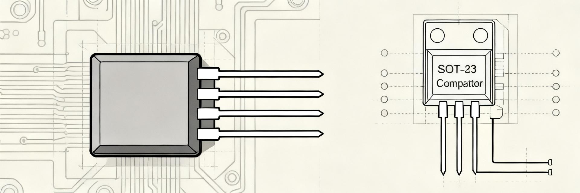
Point: Understanding the pinout is essential for wiring, decoupling, and ESD protection. Evidence: The package used is a small DCK (SOT-23-5/SC-70 equivalent) with standard pins for inputs, output, VCC and GND. Explanation: Map pins explicitly to avoid routing mistakes and place bypass caps close to VCC and GND for stable operation.
| Pin No. | Name | Function |
|---|---|---|
| 1 | IN+ | Non-inverting input — signal sense |
| 2 | IN− | Inverting input — reference or second signal |
| 3 | GND | Ground — connect to clean ground plane |
| 4 | VCC | Positive supply — bypass close to pin |
| 5 | OUT | Output — push-pull/open-drain depending on variant |
Actionable detail: route IN+ and IN− as short matched traces, keep OUT away from sensitive analog traces, and place a 0.1 µF ceramic bypass within 1–2 mm of VCC to GND. If the package has a thermal pad, tie it to ground plane per footprint recommendations.
Recommended PCB footprint & placement tips
Point: PCB layout impacts comparator stability and measured performance. Evidence: Small packages are sensitive to supply and input trace inductance; the datasheet emphasizes bypass placement. Explanation: Place bypass capacitors directly at VCC pin, use a local ground stitch, route inputs with short, low-capacitance traces, and consider ESD diodes on exposed signal lines in harsh environments.
- Bypass: 0.1 µF ceramic + 1 µF bulk near VCC.
- Inputs: keep traces <10 mm where possible; avoid long parallel runs.
- Outputs: use series resistor (50–100 Ω) if driving long traces or to isolate load capacitance.
Electrical Specs & Performance (Datasheet Deep-Dive)
Key absolute/max ratings and recommended operating conditions
Point: Know absolute and recommended limits before bench evaluation. Evidence: The datasheet provides VCC range, input common-mode, differential limits, and temperature ranges. Explanation: Typical operating supply spans low-voltage rails; ensure input voltages do not exceed VCC and pin current limits to prevent latch-up or damage—confirm thermal derating when ambient rises.
| Parameter | Typical / Max | Test Conditions |
|---|---|---|
| Supply Voltage (VCC) | 2.7 V — 5.5 V | Specified range in recommended conditions |
| Input Common-Mode | Rail-to-rail | Within VCC range; check negative headroom |
| Junction Temperature | -40°C to device limit | Refer to thermal tables in datasheet |
Dynamic performance: speed, hysteresis, output drive
Point: Dynamic specs determine signal fidelity and timing margins. Evidence: Datasheet timing shows propagation delay typical hundreds of ns to low µs, rise/fall times dependent on load, and limited internal hysteresis. Explanation: Compare numbers at specified test conditions (VCC, RL to VCC or GND, CL). If the output is push-pull, it can source/sink several milliamps; open-drain variants require proper pull-up choice and consideration of pull-up speed.
Comparator Characteristics & Application Guidelines
Typical application circuits & biasing notes
Point: Two compact circuits cover common needs. Evidence: Standard threshold comparator with pull-up and an open-drain arrangement are well supported by the pinout and output type. Explanation: Use resistor ranges 10 kΩ–100 kΩ for thresholds; place 0.1 µF decoupling adjacent to VCC. For open-drain outputs, choose pull-up voltage consistent with logic domain and consider series resistance for EMI control.
- Single-ended threshold: IN+ to sensor signal, IN− to divider reference, OUT with pull-up to logic rail.
- Open-drain use: OUT to pull-up resistor (4.7 kΩ typical) to required logic voltage, useful for level translation or wired-OR.
Noise, offsets, and temperature behavior — what to simulate/test
Point: Offset and noise define detection accuracy over temperature. Evidence: Datasheet includes offset vs. temperature and propagation vs. supply plots. Explanation: Use the typical curves in SPICE or margin simulations: run input-offset vs. temp and propagation delay vs. VCC to size hysteresis or input filtering. Account for input bias currents when using high-value divider networks.
Example Use Case (Case Study)
Automotive sensor threshold example (or industrial alternative)
Point: Apply the part to an automotive sensor threshold. Evidence: Required threshold at 0.5 V with 3.3 V system and 1 kΩ source impedance yields predictable timing per datasheet propagation. Explanation: Wire IN+ to sensor, IN− to 0.5 V reference divider (10 kΩ/20 kΩ as example); OUT uses 4.7 kΩ pull-up to 3.3 V. Expect propagation in the datasheet range and verify under expected load and temperature.
Bench test checklist & measurement notes
Point: Measured behavior can deviate due to setup. Evidence: Oscilloscope probe capacitance and ground leads alter rise times and can inject oscillation. Explanation: Use ground-spring probe tips, place scope ground as close to device ground as possible, add small series resistor on output if ringing occurs, and capture input and output with identical probe attenuation for timing validation.
- Setup: 0.1 µF bypass at VCC, sensor source impedance known, CL specified.
- Measurements: probe ground spring, use 10× probes, record propagation and rise/fall times at stated RL and CL.
Design Checklist & Troubleshooting (Actionable)
Pre-selection checklist
Point: Quick verification before committing to the part reduces redesign. Evidence: Datasheet sections list supply range, input common-mode, timing, output type, and thermal data. Explanation: Confirm supply compatibility, input range includes expected signal extremes, propagation delay meets system timing, output fits the logic domain, and package/pin footprint matches PCB constraints.
Quick troubleshooting tips
Point: Common issues have quick fixes. Evidence: Oscillation, stuck outputs, or excessive offset are recurring symptoms in comparator circuits. Explanation: If output stuck, verify pull-up and supply; if oscillation occurs, add hysteresis (small feedback resistor) or 1–10 pF across inputs; if offset is large, lower source impedance or add offset calibration in software.
Summary
TLV1831QDCKRQ1 provides a compact, high-speed comparator solution with rail-to-rail inputs and performance suited to fast threshold detection in low-voltage systems. Its small package and clear pinout simplify integration, while designers must watch supply decoupling, input routing, and load conditions to meet timing and accuracy targets; consult the full datasheet for exact test conditions and thermal limits when finalizing designs.
Key Summary
- Pinout & layout: Short input traces, bypass 0.1 µF at VCC, and isolate outputs; this ensures stable operation and predictable timing per the datasheet.
- Critical specs: Verify supply range, input common-mode, and propagation delay against system timing; these define whether the part meets real-time thresholds.
- Application notes: Use 10 kΩ–100 kΩ threshold resistors, 4.7 kΩ pull-ups for open-drain, and expect propagation in the datasheet’s stated test conditions.
- Testing: Use ground-spring probe technique, small series output resistance for capacitive loads, and simulate offset vs. temperature from the datasheet curves.
Common Questions
What is the TLV1831QDCKRQ1 pinout for quick wiring?
The TLV1831QDCKRQ1 features a standard 5-pin SC-70 / SOT-23-5 (DCK) pinout: Pin 1 (IN+) is the non-inverting input, Pin 2 (IN-) is the inverting input, Pin 3 (GND) is ground, Pin 4 (VCC) is power, and Pin 5 (OUT) is the comparator output.
Which datasheet spec most affects propagation delay in practice?
Propagation delay is highly dependent on supply voltage (VCC), overdrive voltage, and load conditions (both load resistance RL and capacitive load CL). Higher overdrive voltages and lower load capacitance significantly minimize propagation delays.
How should I test the TLV1831QDCKRQ1 for automotive sensor thresholds?
Configure the comparator with a calculated reference divider on one input and the sensor on the other. Use a high-bandwidth oscilloscope with ultra-short ground-spring probes to minimize parasitic inductance, and monitor propagation delays across temperature extremes (-40°C to +125°C).
What are the primary troubleshooting steps for comparator output oscillation?
Output oscillation is typically resolved by adding hysteresis via a high-value feedback resistor (e.g., 100kΩ to 1MΩ) from OUT to IN+, placing a 0.1µF decoupling capacitor extremely close to the VCC/GND pins, and keeping signal input traces as short as possible to minimize parasitic feedback paths.





