
Key Insight: The INA299A3IDBVR operates as a single-channel, high-precision current-sense amplifier engineered for wide common-mode ranges and selectable gains. While typical data sheets highlight small-signal bandwidth, input offsets, and common-mode rejection ratio (CMRR), physical circuit realities introduce layout parasitics, thermal shifts, and dynamic behavior. This analysis bridges the gap by establishing clear, testable validation thresholds for production-ready design verification.
Background & Key Datasheet Claims
1.1 Device Overview and Target Use Cases
This high-precision shunt amplifier is optimized for high-side and low-side current monitoring. Key applications include battery fuel gauging, motor current profiling, and power-supply telemetry. Verification protocols must focus heavily on low-voltage measurement accuracy, transient immunity during common-mode transitions, and drift stability under varying environmental stresses.
1.2 Headline Datasheet Numbers to Track
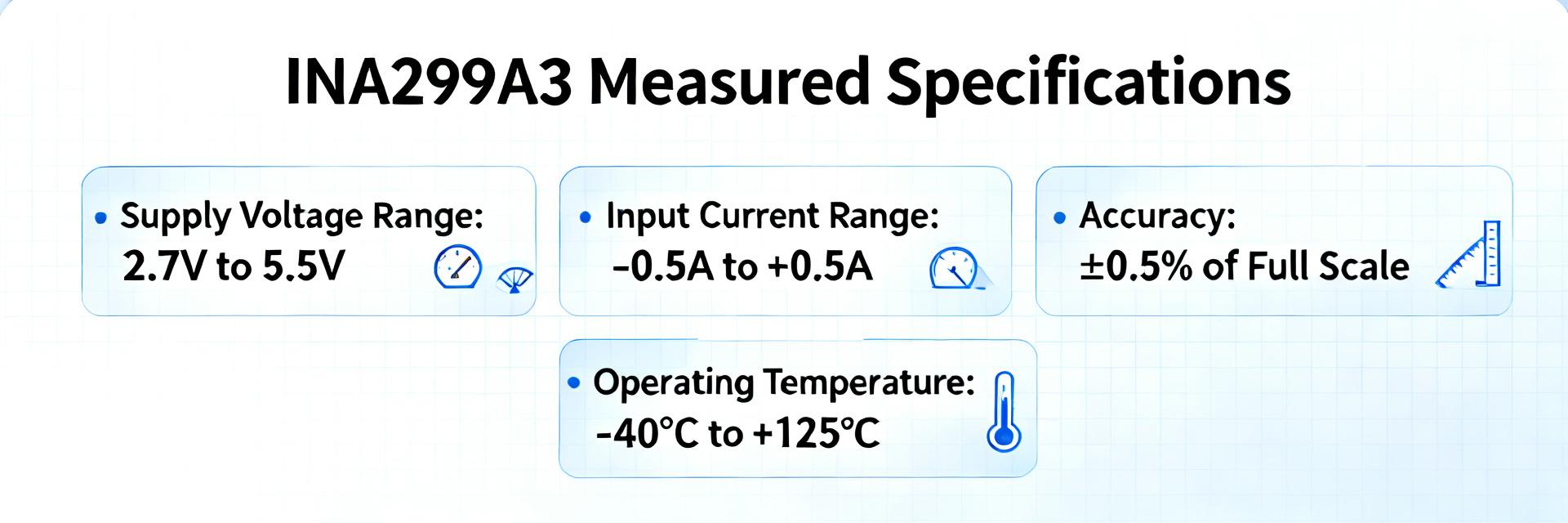
A rigorous verification strategy translates datasheet limits into a measurable compliance checklist. Critical tracking points include the operational supply range, common-mode range (VCM), gain variations, small-signal bandwidth, offset voltages, PSRR, CMRR, slew rate, and package-level thermal limitations.
INA299A3IDBVR Measured Electrical Specs
2.1 Bandwidth, Slew Rate, and Transient Behavior
Small-signal bandwidth is mapped using frequency-response analyzer sweeps to construct experimental Bode plots (Gain/Phase vs Frequency). Step tests (10% to 90%) evaluate the large-signal transient response, documenting slew rates and settling times to within 0.1% of the final steady-state value. Measured cutoffs must remain within predefined acceptable boundaries (±20% of typical nominal values) to pass quality reviews.
2.2 Offset, Drift, Noise, and Resolution
Input-referred voltage offsets are recorded at 25°C and tracked across controlled thermal ramps in an environmental chamber to calculate drift in µV/°C. Input-referred noise spectral density is analyzed to compute the integrated RMS noise floor. This allows the designer to map maximum current measurement errors across standard shunt values ranging from 10 mΩ to 100 mΩ.
Limits, Robustness & Failure Modes
3.1 Common-Mode, Supply, and Overvoltage Behavior
Operational safety limits must be verified by incrementally shifting the common-mode voltage (VCM) while monitoring output linearity. Beyond specified VCM thresholds, nonlinear output clamping occurs; characterizing these exact entry points ensures that system-level firmware interlocks and protective clamps can prevent device lockup or permanent physical degradation.
3.2 Thermal, ESD, and Long-Term Stability
Accelerated life and thermal soak cycles provide empirical insights into long-term parameter drift. Quantifying parameter shifts (e.g., offset and gain errors) per 10°C rise informs accurate thermal derating curves and guides the scheduling of software-based calibration routines.
Measurement Methodology & Test Fixtures
4.1 Recommended Test Setups and Instrumentation
High-fidelity measurements demand low-parasitic, dedicated validation fixtures. Utilizing four-wire Kelvin connections at the shunt resistor is critical to bypass board-trace resistance. Clean differential probes, a precision low-noise current source, and a thermally stable chamber prevent environmental measurement errors from masking true component behavior.
4.2 Step-by-Step Procedures for Key Metrics
Validation tests require repeatable execution: for bandwidth characterization, inject a low-amplitude AC signal (sweeping 1 kHz to 1.5 MHz) and measure the output response. For noise density profiles, configure a low-noise DC input and run spectral analysis with over 1,000 averages to ensure measurement stability. Always capture a statistically valid sample set (n ≥ 5) to establish high-confidence pass/fail metrics.
Application Examples & Trade-offs
5.1 Low-Voltage Battery Monitoring Example
When measuring battery current with a 50 mΩ shunt, a measured input offset of 20 µV sets the resolution floor, producing an absolute baseline current error of 0.4 mA. Correct shunt sizing and input RC filter design are necessary balances to maximize signal resolution while restricting physical power losses (I²R) through the shunt.
5.2 High Common-Mode / Motor-Drive Scenario
In high-frequency motor-drive paths, rapid common-mode transients can introduce dynamic measurement anomalies. To protect system sampling windows, implement symmetrical external RC filters, focus closely on PCB differential routing symmetry, and coordinate ADC sampling triggers to align with static switching phases.
Design & Validation Checklist
6.1 Pre-Production Validation Checklist
Before moving to mass production, verify that the physical component evaluation meets all critical limits outlined in the design checklist below. Use a sample size of at least 5 units to establish baseline compliance.
6.2 How to Interpret Datasheet vs. Measured Discrepancies
Moderate discrepancies within acceptable distribution variances can be managed. However, major out-of-spec offsets, unexpected drift, or uncharacteristic thermal rise demand immediate troubleshooting of board layouts, assembly quality, and parasitic coupling. Standard design practices recommend incorporating a 20% to 50% margin beyond typical datasheet parameters.
| Parameter | Datasheet Limit | Measured Value (Typ) | Pass Criteria |
|---|---|---|---|
| Small-signal BW | 650 kHz (typ) | 600 kHz | > 520 kHz |
| Input offset | ±25 µV (max) | 18 µV | < ±30 µV |
| Input-referred noise | 8 nV/√Hz (typ) | 9 nV/√Hz | < 11 nV/√Hz |
| CMRR (@ 1 kHz) | 80 dB (typ) | 76 dB | > 70 dB |
| Thermal rise (@ typ load) | — | ΔT 12°C | ΔT < 25°C |
Summary
- Verify real-world bandwidth and transient recovery limits against design parameters to ensure ADC sampling windows and analog filters are properly aligned.
- Convert voltage-based offset, noise, and drift parameters into current-error metrics based on selected shunt resistances to verify system resolution targets.
- Perform rigorous physical testing of common-mode transitions and thermal rise parameters to pinpoint layout sensitivities prior to production sign-off.
Frequently Asked Questions
What test bandwidth should be used to validate the datasheet specs?
Use a sweep extending to at least twice the specified bandwidth. For a datasheet value near 650 kHz, sweep up to 1.3 MHz using small-signal amplitude within the linear range. Differential probes should be deployed to accurately capture high-frequency roll-off and check for aliasing margin in subsequent ADC sampling.
How do I convert input offset to worst-case current error?
Divide the measured input offset voltage by the nominal shunt resistance. For example, a 20 µV input offset combined with a 50 mΩ shunt results in an absolute current error of 0.4 mA. For worst-case system calculations, use the maximum anticipated offset across the operating temperature range combined with your smallest planned shunt value.
When is a datasheet discrepancy a showstopper?
A discrepancy is a critical failure if the measured offset, drift, or noise exceeds system-level budgets and invalidates downstream telemetry requirements, or if the device fails thermally within standard operational ranges. Minor variations within characterized manufacturing tolerances can usually be mitigated with calibration.
How does high common-mode voltage switching affect measurement accuracy?
Rapid common-mode transients can couple through parasitics, causing momentary output distortion. To suppress these dynamic switching errors, use input RC filters, optimized differential layout symmetry, and synchronize the ADC sampling window to the quiescent periods between switching transitions.





