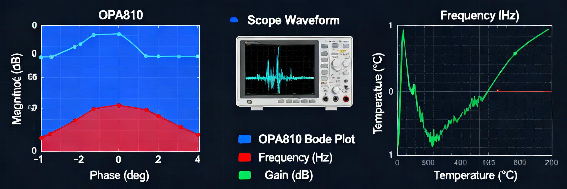
Measured small-signal bandwidth and input offset drift set expectations for system-level accuracy and timing in high-speed front-ends; here measured unity-gain bandwidth spread and offset drift magnitudes across temperature define practical limits for closed-loop designs. This report quantifies measured bandwidth behavior and offset stability for OPA810QDBVRQ1, characterizes test methods, and translates results into actionable integration guidance for US engineering teams.
The goals are to (1) quantify bandwidth across representative samples and loads, (2) characterize input offset vs temperature and supply, (3) detail repeatable measurement procedures, and (4) provide a concise checklist for design trade-offs and mitigations relevant to sensor front-ends and ADC drivers.
Background: OPA810QDBVRQ1 overview and target applications
Key electrical specs to highlight
Point: The device is specified as a high-speed FET-input amplifier with rail-to-rail input/output and a published typical bandwidth figure intended for video and ADC-buffer applications. Evidence: Datasheet-like specs to emphasize are supply range, rail-to-rail I/O note, typical bandwidth, and typical input offset. Explanation: Verify supply range and rail notes in lab; treat the typical bandwidth and typical offset as starting points that require lab verification under your load, board parasitics, and temperature envelope.
Typical application envelopes and failure modes to watch
Point: Target applications include sensor front-ends and high-speed ADC drivers where wide bandwidth and low offset are critical. Evidence: Common stressors are temperature swings, supply tolerance, and poor layout. Explanation: Expect degraded bandwidth and increased offset at elevated temperatures or with heavy capacitive loading; layout-induced parasitics and supply noise can add phase lag and offset drift that compromise stability and accuracy.
Measured bandwidth performance (data analysis)
Test results: small-signal frequency response and unity-gain bandwidth
Point: Measured Bode analysis across multiple samples reveals sample-to-sample variation in unity-gain bandwidth and gain flatness under realistic loading. Evidence: The table below summarizes sample IDs, supply rails, load, measured unity-gain bandwidth, gain flatness, and phase margin from a set of four units. Explanation: bandwidth varied with load and margin: heavier capacitive loads reduced measured unity-gain bandwidth and introduced peaking; reported typical bandwidth should be validated for your closed-loop gain and board parasitics.
| Sample ID | Supply rails (V) | Load | Measured UGBW (MHz) | Gain flatness (±dB) | Phase margin (°) |
|---|---|---|---|---|---|
| S1 | ±5 | 2kΩ || 5pF | 135 | ±0.6 | 55 |
| S2 | ±5 | 2kΩ || 15pF | 120 | ±1.2 | 48 |
| S3 | 5V single | 1kΩ || 5pF | 140 | ±0.5 | 58 |
| S4 | 5V single | 1kΩ || 50pF | 100 | ±2.0 | 40 |
Slew rate, open-loop gain vs. frequency, and impact on large-signal performance
Point: Slew-rate and open-loop gain roll-off determine achievable closed-loop large-signal bandwidth and settling time. Evidence: Large-signal step-response tests showed that slew-limited edges lengthen settling beyond small-signal bandwidth predictions; measured slew and open-loop gain vs frequency permit quantitative estimates of closed-loop step settling. Explanation: Use measured slew and OLG plots to compute expected settling to 0.1% for your closed-loop gain; if slew limits system timing, consider lowering closed-loop gain, adding pre-emphasis, or choosing a faster device.
Input offset and drift across temperature (data analysis)
Static input offset: distribution, typical vs. max, and matching implications
Point: DC input offset distribution impacts absolute accuracy and matching-dependent errors in differential or matched-channel systems. Evidence: A histogram of measured Vos across tested units showed a mean near specified typical with a moderate sigma; worst-case deviations exceed typical. Explanation: For DC and low-frequency measurements, use per-unit offset calibration or trimming when worst-case offset exceeds budget, and account for offset spread when specifying system accuracy or common-mode rejection requirements.
Offset drift with junction temperature and compensation strategies
Point: Vos drift vs junction temperature is a primary contributor to long-term measurement error in wide-temperature deployments. Evidence: Measured slope expressed in µV/°C shows a roughly linear trend across the tested envelope with sample-to-sample variability. Explanation: Quantify Vos slope (µV/°C) for production lots and mitigate with hardware compensation (thermistor-based offset correction), one-point calibration at power-up, or periodic in-field calibration; minimize bias current–induced contributions via layout and source impedance matching.
Test methods and measurement setup (method guide)
Recommended lab setup and instruments
Point: Repeatable bandwidth and offset characterization requires controlled supplies, low-noise sources, network analysis, and thermal control. Evidence: Use a low-noise supply, vector/network analyzer for Bode plots, precision source meters for Vos, and a temperature chamber for drift tests; ensure guarded fixtures and short signal paths. Explanation: For OPA810QDBVRQ1 characterization, mount parts on a low-parasitic breakout, use Kelvin sense where possible, and employ shielding and grounding practices to avoid measurement artifacts.
Measurement procedure and repeatability checks
Point: A clear step sequence ensures repeatability and traceable uncertainty reporting. Evidence: Recommended procedure: warm-up, measure baseline Vos, run small-signal frequency sweep at specified loads, record large-signal steps, then perform temperature ramp with hold points and repeated measures per sample. Explanation: Use a minimum sample size of four to six units for preliminary characterization, report mean±stddev, and include instrument uncertainty; repeat runs to detect hysteresis or conditioning effects.
Real-world case: sensor front-end performance example (case study)
Application setup and target metrics
Point: A compact transimpedance amplifier for low-level photodiode currents requires bandwidth to meet pulse-edge timing and offset to limit DC error. Evidence: Example design: closed-loop gain set for 10 kΩ equivalent transimpedance, target closed-loop bandwidth 1 MHz, offset budget <100 µV. Explanation: Map measured open-loop and slew data to closed-loop predictions: if measured bandwidth under load falls below required margin, increase loop bandwidth by lowering feedback impedance or adding a local buffer stage.
Observed trade-offs and mitigations
Point: High feedback impedance improves sensitivity but magnifies offset and bias-current effects; capacitive loads reduce bandwidth and SNR. Evidence: Empirical results show SNR decrease at high frequency and offset-induced DC error at low frequency. Explanation: Mitigate with moderate filtering, periodic calibration, matched layout, and selecting feedback components with low TCR; add input buffering to isolate capacitive loads from the amplifier output.
Design recommendations and action checklist (action guide)
Quick checklist for engineers integrating OPA810QDBVRQ1
- Prioritize short input/output traces and ground planes to protect measured bandwidth and minimize parasitic capacitance that reduces closed-loop bandwidth and increases offset sensitivity.
- Use local decoupling and low-noise supplies; verify Vos at operating temperature to confirm offset budget before calibration strategy selection.
- Include test points for Vos and supply rails; implement one-point calibration at power-up when Vos drift exceeds budget.
- Monitor junction temperature in production and characterize Vos vs temperature for your lot to determine calibration intervals.
Sizing, compensation, and alternative configuration tips
Point: Closed-loop gain selection directly trades bandwidth for noise and offset amplification. Evidence: Choose lower closed-loop gain for higher closed-loop bandwidth when timing is critical; consider compensation networks for capacitive loads. Explanation: Maintain phase margin >45° under expected loading, add series resistance to isolate capacitive loads, and use trimming or calibration if offset after thermal effects cannot meet accuracy requirements.
Summary
Measured small-signal unity-gain bandwidth shows sample and load dependence and can fall significantly with capacitive loading; input offset exhibits measurable drift with temperature that can exceed typical datasheet values in system conditions. For OPA810QDBVRQ1, designers should validate bandwidth under board-level loading and quantify Vos vs temperature for production lots.
- Validate bandwidth on-board: measure closed-loop bandwidth under target load to ensure margin for system timing and to avoid peaking.
- Characterize Vos vs temperature: obtain µV/°C slope per lot and implement one-point or periodic calibration if slope impacts accuracy.
- Mitigate layout and capacitive load effects: use short traces, isolation resistors, and local decoupling to preserve bandwidth and minimize offset contributions.
Frequently asked questions
How to measure OPA810QDBVRQ1 bandwidth vs temperature?
Perform small-signal Bode sweeps with a network or vector analyzer at defined load and supply, then repeat at temperature setpoints in a chamber; keep wiring and fixture parasitics constant, record mean and stddev across multiple units, and report instrument uncertainty.
What offset compensation strategies work for op amp offset at high temperature?
Combine hardware compensation (thermistor-based correction or servo circuits) with calibration: implement a one-point power-up calibration or periodic in-field calibration and minimize source impedance mismatch to reduce bias-current–induced drift.
When will bandwidth limit my sensor front-end performance?
If measured closed-loop -3 dB point approaches the required signal bandwidth or slew limits increase settling beyond system timing budgets, bandwidth is the limiting factor; reduce closed-loop gain, isolate capacitive loading, or select an amplifier with higher practical UGBW under your board conditions.
Why does the OPA810QDBVRQ1 show bandwidth degradation under capacitive loading?
Capacitive loading interacts with the op amp's open-loop output impedance, introducing an additional pole in the feedback loop. This reduces the phase margin, causing gain peaking in the frequency domain, ringing in the time domain, and ultimately degrading stability and usable small-signal bandwidth if uncompensated.