
Typical lab anchors for this classic small-power audio IC show THD+N near 0.015% at 1 kHz for a clean 20 W condition, and reliable 20 W delivery into both 4 Ω and 8 Ω loads on mid-range bipolar rails. Measured headroom scales with supply voltage; thermal limits and gain setting govern maximum continuous output.
This report covers a concise specs recap, an electrical deep-dive, reproducible bench methodology, measured results for power, THD, SNR, frequency response and thermal rise, plus practical board-level and component recommendations aimed at US engineers and hobbyists seeking actionable test conditions rather than marketing claims.
LM1875T at a Glance: Key Specs and Typical Performance
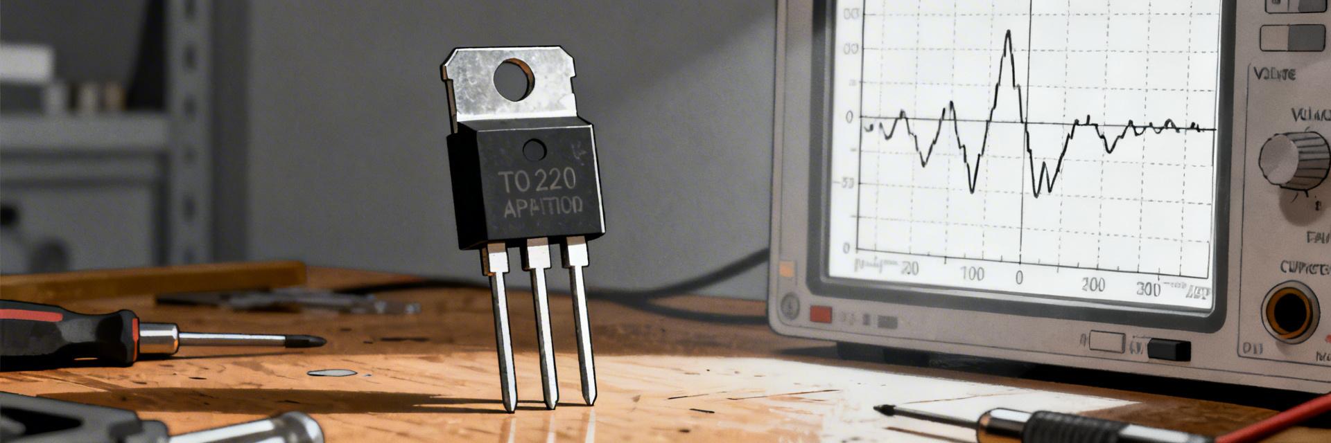
Device Overview & Electrical Highlights
Core device points: single-ended audio power amplifier in a TO-220 style package offering ~20 W continuous per channel into 8 Ω under typical datasheet rails, THD+N quoted at ~0.015% (1 kHz, 20 W), SNR in the high 80s to low 90s dB depending on gain, and recommended bipolar supply ranges for stable operation. Typical vs. maximum ratings are distinct—design to typical for sonic expectations and to absolute max for reliability.
| Parameter | Headline Value |
|---|---|
| Rated output | ~20 W into 8 Ω (typical test rails) |
| THD+N | ~0.015% at 1 kHz, 20 W (typical) |
| SNR (ref full scale) | ~88–92 dB (gain dependent) |
| Supply range | Bipolar rails, practical ±18 V to ±30 V |
Typical Application Circuits & Recommended Operating Envelope
Standard application uses a single amplifier per channel with local input coupling, input resistor/gain network, and output coupling or bridge config as needed. Typical loads are 4 Ω and 8 Ω; decoupling and supply bypass close to the package are essential. Expect lower measured power with non-ideal supplies and elevated THD near clipping or under thermal stress.
Electrical Specifications Deep-Dive
Power Output, Gain Structure, and Load-Dependent Behavior
Output power is best estimated from Vrms and load: P = Vrms² / Rload. Vrms depends on rail headroom and device saturation; usable Vrms ≈ (Vrail − Vdrop)/√2 for conservative estimation. Raising gain reduces required input voltage for a given output but narrows margin to clipping. Non-ideal supplies (droop, ripple) reduce continuous power versus datasheet figures.
Distortion, SNR, and Frequency Response Characteristics
THD+N is lowest at midband low-to-moderate outputs and rises approaching clip and at high frequencies. Measure at 1 kHz at representative power points (1 W, 10 W, near-clip) and sweep 20 Hz–20 kHz for frequency response. SNR depends on gain and input coupling; aim for higher closed-loop gain only when required and keep input source noise low.
Benchmarks: Lab Setup and Test Methodology
Test Bench & Equipment
- FFT-capable audio analyzer / ADC
- Precision dummy loads (4Ω/8Ω)
- Regulated dual rails (±18V to ±30V)
- A-weighting & 20Hz-20kHz filters
Sample Selection & Anti-Bias
Test multiple ICs and PCB builds to capture variance. Apply thermal stabilization runs before capture, log ambient conditions, and randomize test order to avoid systematic bias. Present error bars for sample spread.
Measured Benchmarks: Results and Interpretation
Key plots should include Power vs. THD at 1 kHz, THD vs. Frequency at 1 W, 10 W and near-clip, and a flatness sweep 20 Hz–20 kHz. Expect datasheet anchors like ~0.015% THD at clean 20 W to be a realistic target under controlled conditions; deviations upward are common with supply ripple, poor decoupling, or conservative heat management.
Practical Recommendations for Designers and Hobbyists
PCB Layout & Decoupling
Prioritize short, wide output traces, single-point star ground for sensitive inputs, and place decoupling caps (100 nF ceramic + 10–100 µF electrolytic) within millimeters of power pins. Add a 220 µF bulk cap in the supply return and use low-ESR parts.
Load & Heatsinking
Match speaker impedance and enclosure tuning; choose heatsink area proportional to expected continuous dissipation. If noise or oscillation occurs, increase input capacitance, add small series resistors at inputs, and verify ground returns.
Common Questions
How should I set up a test to measure THD and power reliably? +
What heatsinking approach prevents thermal limiting? +
Which common layout errors most often increase THD or cause oscillation? +





